>> TechXchange: Chip Packaging
Download this article in .PDF format
What you will learn
Chip die sizes continue to grow, as does the number of connections. The switch to high-speed serial interfaces reduced the required pin count, but that simply slowed the pin count down.
Dual inline packages (DIPs) used to be the mainstay for the electronics industry, and many applications still use them. They worked well with sockets and circuit boards. Through-hole connections allowed double-sided and then multilayer boards.
The problem is that DIPs hit limitations as they scaled down in size and the number of connections rose. These days, surface-mount technology (SMT) has become the primary way to utilize electronic components.
Inside The Chip
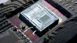
The die inside a chip are much smaller than the chip. A lead frame typically surrounds the die. Early microcontrollers were delivered in packages as large as 40 pins like the 8-bit Intel 8742 (Fig. 1). The die has a large bonding pad. A bonding wire connects the pad to a lead in the lead frame that is the pin on the exterior of the chip.
Related Articles
- The Tiny Corex-M0+ Just Got Smaller
- Apple Rolls Its Own Dual-Core A6 For The iPhone 5
- Hybrid Memory Cube Shows New Direction For High-Performance Storage
- The Fundamentals Of Flash Memory Storage
DIPs limited the size of pins, but the approach still works for some surface-mount packages. For example, flat-pack packages are internally similar to the technology used on the 8742, but the exterior pins were designed for surface mounting. Dual and quad flat-pack (QFP) chips are now very common for surface-mount applications.
Leadless chip carriers (LCCs) essentially eliminate the leads but keep the same internal architecture. The connections are exposed on the bottom and sometimes the side of the chip. These chips allow denser circuit boards. Some LCC form factors can be mounted in matching sockets. These form factors typically were processors or more expensive components.
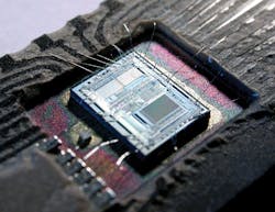
A single lead frame does not work well with chips that sprout hundreds of pins. A move to stacked frames like the ones used in Intel’s Pentium allows more bonding wires to be connected in a smaller area (Fig. 2).
Ball grid arrays (BGAs) place the chip on top of a double-sided circuit board (Fig. 3). The bonding wires on top of the die connect to a small, double-sided circuit board. Solder balls are attached to the bottom of the board, and through-holes link the balls to the pads connected to the gold bonding wires.
Chip And Wafer Scale Packaging
BGAs are moving toward chip-scale packaging (CSP), where the die size is very close to the package size. In some cases there are cooling and power challenges.
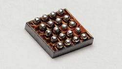
Wafer-scale packaging eliminates the BGA circuit board and attaches the solder balls directly to the die (Fig. 4). Freescale’s Kinetis KL02 uses this approach (see “The Tiny Corex-M0+ Just Got Smaller” at electronicdesign.com).
This 48-MHz, 32-bit Arm Cortex-M0+ microcontroller fits into a 1.5-mm by 2-mm package (Fig. 5). The chip is so small, it can be used in medical devices that would be swallowed. Of course, using only 36 µA/MHz helps keep power requirements down as well.
A package usually includes a single die. This simplifies the overall design, and it’s normally the configuration required for a chip. A larger die can address higher-density applications.
Unfortunately, moving to a larger die is not always an option. In other instances, multiple dies may be required because each die needs to be created separately. This is often the case when different technologies are required. For example, some analog or power circuits are better when they are not built on the same die as the digital components.
There are several ways to create a system-in-package (SiP), not to be confused with single inline packages (SIPs), which are simpler DIPs. Multichip SiPs come in a number of forms where multiple die can be blended in one package. We will take a look at 3D die later. 3D tends to be a much different approach than simply packaging die together.
Multichip carriers enable designers to put more than one die into the package. There are numerous multichip solutions, but in general they employ a circuit board to connect the chips together and to link them to the pins or solder balls.
Multichip carriers give designers a common pin-out but utilize different dies, possibly to provide faster processors or more memory. These chips often are used to combine processor and support chipsets so a system-on-chip (SoC) can fit into a single chip. Intel has taken this approach with a number of chips, and the company is not alone.
Another way to mix multiple chips together is to stack them on top of each other (Fig. 6). The dies are not the same size, so the bonding wires can be attached to each die.
Not all die can be stacked, but the approach has proven very popular with mobile devices. Smart phones and tablets often require stacked solutions to address their small size. Apple’s A4 and A5 SoC solutions for the iPhone and iPad add a memory die on top of the dual-core processor (see “Apple Rolls Its Own Dual-Core A6 For The iPhone 5” at electronicdesign.com).
Multichip carriers and stacked die each have challenges. They are more complex to build and require exacting standards. Power distribution and heat distribution are also significant issues in most applications. The issues depend upon the chips employed and how they are utilized.
For example, multichip carriers like those used with high-end microcontrollers have die that dissipate considerable amounts of heat. Separating them in a multichip carrier enables better heat distribution to heatsinks. A stacked die would be a challenge because the heat dissipation also can affect how the die are mounted.
Stacked die will generate heat, which must be kept within a manageable range. That’s why a smart phone can get rather warm, but it shouldn’t get as hot as a processor chip within a PC.
Two-level stacked die are common. Multilevel stacked die are possible, but additional levels increase system complexity. Construction obviously requires more steps.
Multichip packages have other advantages. Each die in a package can be tested and verified prior to package construction. This makes it more likely that the package will result in a working system. Likewise, die can be binned (categorized) based on functionality and performance.
Multichip packages reduce wiring distances. Wiring density, although less than on-chip, normally is higher than off-chip wiring density. Likewise, the in-package wiring can be more efficient. It also is not as susceptible to the printed-circuit board (PCB) design. High-speed serial connections and parasitic capacitance issues tend to exacerbate these issues.
Multichip solutions are becoming more common because of the variety of technologies needed these days. Nanotechnology is often utilized for sensors like accelerometers. Developers are also looking for smart sensors and matching them up with a microcontroller. Mixing multiple sensors with the microcontroller allows sensor integration in a single package.
Going Past 2D
Multichip solutions result in more dense packages, but moving toward the die in terms of design can reduce size further while increasing connection density. This is important in a number of applications.
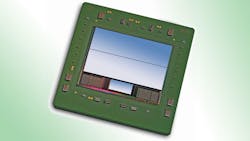
Xilinx’s 2.5D technology takes this approach (Fig. 7). It utilizes a 65-nm metallic interposer layer to connect up to four dies or “slices.” The slices can be homogeneous or heterogeneous.
The Virtex-7 H580T employs two 28-nm FPGA slices and a high-speed serializer-deserializer (SERDES) slice with eight 28-Gbit/s transceivers implemented in 40-nm technology (Fig 8). The SERDES can be mixed with the FPGA slices, but the result is suboptimal in terms of performance and efficiency. The hybrid approach provides the best of both silicon technologies.
The interposer provides a significantly higher slice-to-slice interconnect density that would be possible using bonding wires that are in turn better than doing the same thing off-chip. There are tens of thousands of connections between slices.
Improving the design tools was paramount in producing FPGA designs that take advantage of the multislice architecture. Xilinx’s Vivado design tool does this (Fig. 9). It knows about the multislice nature of the Virtex-7 as well as how the interconnects link the slices together.
The 2.5D interposer approach is similar to the multichip carrier except on a much smaller, finer scale. The approach works very well with FPGAs that need a high-density slice-to-slice interconnect. This more regular interconnect approach could be applicable to mixing other array-style dies such as memory die including DRAM and flash or other non-volatile storage. Here the wide parallel connects would be more efficient, eliminating the transceivers and SERDES now found in many high-density memory interfaces.
The approach would be more challenging for mixed logic slices since the technology is relatively new. Still, the approach would be a good way to mix a hard-core processing slice with a set of FPGA slices and high-speed SERDES. Nothing like this has been announced yet, and it will be at least a couple of years before it might occur.
3D Memory Stacks
Stacked die are one form of die-on-die packaging technology that has a long track record. Stacked 3D solutions also are emerging. They employ through-silicon vias (TSVs) to create a true 3D chip. They have the advantage in terms of connection density and efficiency, but they do have heat and power distribution issues like the stacked-die approach. Power has to be distributed through the die to the next one above. The same is true for heat.
The 3D stacked chip holds a lot of promise and may eventually be as common as multilayer PCBs are now. For now, memory solutions are taking advantage of this approach.
The Hybrid Memory Cube (HMC) Consortium (see “Hybrid Memory Cube Shows New Direction For High-Performance Storage” at electronicdesign.com) has delivered its first specification, which defines an architecture with a logic layer and multiple, identical memory die stacked on top of it in a 3D TSV configuration (Fig. 10).
The logic layer provides the access mechanism to the memory die and the high-speed serial interface to the outside world. The approach eliminates the bonding wires found in stacked die solutions using TSV for connections between memory chips and to the logic layer. An HMC has four or eight memory die. A board designer will only need to contend with the capacity and standard interface in a fashion similar to DRAM modules today.
There are architectural differences between a DRAM module and an HMC. DRAM modules are designed to work with a single host, although that host may be part of a multicore NUMA system. HMCs are designed to work with multiple hosts and can be employed in an array (Fig. 11). An array of HMCs increases the capacity potential but also the system’s bandwidth potential. A host attached to any point of the array has full access to the entire memory.
Multiport support of a single HMC has design implications for multihost environments such as network switching. It simplifies host memory management and provides scalable support that would otherwise require more complex host designs like those found in high-end, multicore processors.
The multiport HMC interface uses high-speed serial links like PCI Express but with its own HMC protocol. It is scalable by lane like PCI Express, and a single HMC chip can support hosts with different link requirements. The interface is host agnostic, although a host will obviously need an HMC interface. This should be a software design exercise for FPGAs.
HMC represents a major change in memory architectures. It should be able to provide a 15x bandwidth increase compared to DDR3 while cutting power per bit by 70%. The 3D architecture reduces the memory footprint by 90%. Of course, the memory system should have a lower latency and higher availability than existing memory solutions.
Companies like Micron are looking to deliver HMC chips in the near future (Fig. 12). Initially, HMC is targeting high-performance applications such as networking and servers. Thicker chips will stand out in the future, but initially they will be very similar to packages already found on systems. Standard pin-outs will make designing with HMC chips easy with multiple sources for the hardware. HMC hardware will be available in the next year or so.
HMC currently targets DRAM. In the future, it could address non-volatile storage. Designers are already mixing flash and DRAM like Viking Technology’s ArxCis-NV hybrid DDR3 DRAM module, which also incorporates flash backup storage (see “The Fundamentals Of Flash Memory Storage” at electronicdesign.com). It might simply be a matter of adding a flash memory die or two to the HMC stack.
Electronic packages have progressed significantly from early DIPs to 3D stacked memory. Most systems employ a mix of packaging solutions, and many will be with us for decades. High density and high speed aren’t required for all solutions, but the newer packaging solutions come in very handy when they are required.
This file type includes high resolution graphics and schematics.


