When doing designs with FPGA you are guaranteed to run out of routing resources before you use all the cells and registers available. And usually you run out of resources at critical phase of the design where you need to finish the development according to schedules.
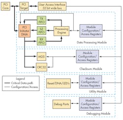
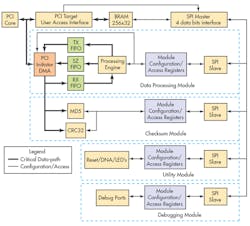
This is how typical design cycle begins. You are approached by your boss and he asks you to build this complex but incredible product/design. You come up with a solution, run few tests, do estimate calculations and create a design using particular FPGA. Before the prototypes arrive you start coding and have about 25% FPGA utilization. Everything is going according to the plan. In my case it was a product that could process gigabytes of data by accessing it via scatter gather DMA engine, calculate the checksum and MD5 while doing it and then put the processed data back into CPU memory through DMA. The solution that I came up with (Fig. 1) uses a 32-bit data bus access as data medium used throughout the design.
The initial design have about 8 registers for DMA configuration/processing in Data Processing Module, 6 registers for Checksum Module, 2 registers for Utility Module and none for Debugging Module (after all who needs debugging, you just turn the power on and everything works like a charm at first try or so I thought).
In reality this design took six months of effort to get fully operational. At this time everything was fine, my FPGA utilization was about 50% at this point and design was progressing according to schedule. Then I was approached by boss again telling me that we need to change the design to add capability to update the FPGA on the field, start - stop the data stream arbitrarily and few other “minor”. improvements. At this time my register count for the design jumped to about 60. The routing engine for FPGA started to take several hours to complete and it was not always successful.
This file type includes high resolution graphics and schematics when applicable.
When my design resource utilization reached about 80% the FPGA routing engine gave up without meeting timing requirements. The routing resources in FPGA are crucial to meet timing requirements for demanding applications and they are the first to deplete. When resource utilization reaches critical levels (70-80%) then the FPGA routing engine is forced to choose non-optimized routes and this adds to propagation delays of routed signals. The last resort for the routing engine is using logical cells for routing and at that time all bets are off and usually the timing results fail miserably.
And sometimes the FPGA routing engine just gives up with a message something along the lines “cannot route due to design complexity”. This happened while expanding our design by adding more functionality. In this case FPGA routing algorithm declared defeat while I was utilizing less than 85% of FPGA. The brute force solution to the problem was simple; just choose an FPGA with bigger cell count and more routing resources. But the price you pay for “simple” brute force approach is additional costs attached to every production unit, new schematics, new layout and new prototype and all that when your project schedule is thrown out of the window. This was unacceptable at many levels and I decided to determine the root cause of these failures and maybe just change my coding style to make the FPGA routing algorithm happy again.
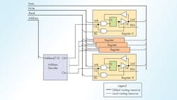
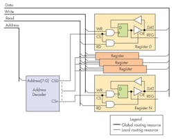
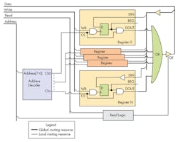
It was obvious from the beginning that FPGA routing algorithm was choking on 32 bit data bus routing and I focused my efforts to analyze this region of design. I was employing simple tristated bus design to implement the register array for configuration/access and simplified coding at high level (Fig. 2). This bus was targeted to have maximum number of registers limited to 256, set by usage of eight bit address bus. Address decoder was selecting the desired register for Read/Write operation into/out of 32 bit D flip-flop. The REG output was used as local variable in the design, providing configuration/command interface. At first glance it seems that we are not using much routing resources, 32 (Data bus) + 1 (Read) + 1 (Write) + 8 (Address) or total of 42 routing terms. I was aware that FPGA does not have internal tristated busses and allowed the FPGA routing algorithm to translate this code into multiplexor based design. Upon closer examination I found that routing engine was mapping my register array (Fig. 3).
Note that this is ideal case and when going gets tough the routing engine start using local cells as routing resource and that case creates much more complications in timing closure, but we are going to analyze only ideal solution. So for N registers we will be using 32 (DIN) + 32 * N (DOUT) + 1 (Read) + 1 (Write) + 8 (Address) or in case of 60 registers we are looking at utilization of 1920 routing terms. In case of full address space utilization (N = 256) we will be using 8202 routing terms.
While this number does not seem high we should consider that usually FPGA designs are much more complex than register array described in Figure 3 and most routing resources are distributed evenly. So if you design/coding is using some concentration of logic, the routing resources will deplete in that region quickly and the resulting mapping will not fit in FPGA, no matter how good is the routing algorithm.
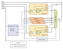
My first attempt at this issue was to help the routing algorithm by eliminating those monstrously large muxes. Figure 4 shows my approach of using large OR gate for muxing DOUT data bus. This was done by assuring DOUT was set to zero when CS is not asserted. This help dissolve the logic employed in muxes in Figure 4 into local resources.
-- General purpose register –
  \library IEEE;
use IEEE.std_logic_1164.all;
entity gen_reg is
  generic(DAT_BITS  : natural := 32;
    AUTOCLEAR : boolean := false;
    AUTOC_VAL : std_logic_vector(31 downto 0):= (others => '1');
    RST_VALUE : std_logic_vector(31 downto 0):= (others => '0');
    ADDR_VALUE  : std_logic_vector(7 downto 0);
    ADDR_BITS : natural := 8);
  port (  din     : in  std_logic_vector (DAT_BITS-1 downto 0);
  dout  : out std_logic_vector (DAT_BITS-1 downto 0);
  rout  : out std_logic_vector (DAT_BITS-1 downto 0);
  addr  : in  std_logic_vector (ADDR_BITS-1 downto 0);
  cs      : in  std_logic;
  wr      : in  std_logic;
  rst     : in  std_logic;
  clk     : in  std_logic);
end entity gen_reg;

architecture rtl of gen_reg is
signal reg_update : std_logic;
signal gen_reg0 : std_logic_vector(DAT_BITS - 1 downto 0);
signal gen_reg1 : std_logic_vector(DAT_BITS - 1 downto 0);
signal gen_reg0_rst : std_logic;
signal autoclr_rst : std_logic;
signal addressed : std_logic;

begin
  process(clk)
  begin
    if(clk'event and clk = '1') then
    if(gen_reg0_rst = '1') then
    gen_reg0 <= RST_VALUE(DAT_BITS - 1 downto 0);
    addressed <= '0';
    reg_update <= '0';
    else
    if((addr = ADDR_VALUE) and (cs = '1')) then
    addressed <= '1';
    if(wr = '1') then
    reg_update <= '1';
    gen_reg0 <= din;
    end if;
    else
    addressed <= '0';
    reg_update <= '0';
    end if;
    end if;
    end if;
  end process;

gen_reg_simple: if(AUTOCLEAR = FALSE) generate
  -- register the value while synchronizing to clk
  process(clk)
  begin
    if(clk'event and clk = '1') then
  if(rst = '1') then
    gen_reg1 <= RST_VALUE(DAT_BITS - 1 downto 0);
  elsif(reg_update = '1') then
    gen_reg1 <= gen_reg0;
  end if;
    end if;
  end process;
  gen_reg0_rst <= rst;
    autoclr_rst <= '0';
end generate;

gen_reg_with_autoclear: if(AUTOCLEAR = TRUE) generate
  -- register the value while synchronizing to clk
  process(clk)
  begin
    if(clk'event and clk = '1') then
  autoclr_rst <= '0';
  if(rst = '1') then
    gen_reg1 <= RST_VALUE(DAT_BITS - 1 downto 0);
  elsif(reg_update = '1') then
    autoclr_rst <= '1';
    gen_reg1 <= gen_reg0;
  else
    gen_reg1 <= gen_reg1 and AUTOC_VAL(DAT_BITS - 1 downto 0);
  end if;
    end if;
  end process;
  gen_reg0_rst <= '1' when (rst = '1') or (autoclr_rst = '1') else '0';
end generate;

rout <= gen_reg1;
dout <= gen_reg1 when (addressed = '1') else (others => '0');

end rtl;
The module gen_reg.vhd (Listing 1) does local address decoding to save global routing resources. It has several parameterized functions to help use this code all over the design without modification. Most of parameters are self explanatory but one parameter, the AUTOCLEAR needs some clarification. This functionality is necessary for registers that act as triggers of events. For example, when we initiate a DMA the run bit of command register, as implemented using gen_reg.vhd, is cleared after one clock cycle. This allows worry free operation of design, in case we forget to clear this bit or DMA cycle finished before we cleared it. We use this register design unchanged in final implementation.
This coding change improved routing algorithm speed but was not successful to solve the overall bottleneck. The end result of this design change was less logic utilization and it speed up the FPGA routing algorithm. The resulting FPGA image was produced much faster but was failing to meet timing constraints.
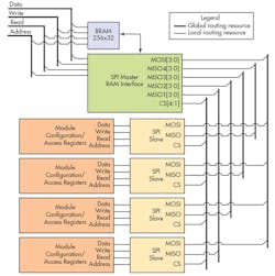
It was clear that the problem requires more detail analysis and radical design changes. Reducing number of configuration registers was not an option, since I was only anticipating the design will just get more complex as it matures. The solution to the routing problem was found in time domain, more specifically in using four bit SPI to simplify it. The critical data path were marked with tick lines in Figure 1. We called it critical since amount of data moved through those paths are several orders of magnitude higher than the data path used for module configuration and accessing operation results. This presented us with opportunity to serialize module communications with minimal impact on design performance (Fig. 5).
I used dual port ram as configuration memory and to store results of operations. This RAM contained copy of all the configuration/results that each module registers have. At first we arranged that this configuration buffer was refreshed automatically but quickly realized it is much easier to synchronize with software if we do it under software control. This way software would configure the memory and instruct the SPI Master to transfer/refresh the module registers. In this case we are using 20 wires for data path (4 out and 16 in) from SPI master and by using 256x32 memory we have enough space to address 256 registers.
This approach to the design saved routing resources and gave us room to complete the design with existing FPGA platform and eliminate the need to redesign hardware. Currently we are utilizing more than 85% of FPGA and routing engine is happily doing its job. The finished design is shown in Figure 6. We settled in using four modules and assigning each module 64 register configuration space. We are running the SPI bus at 33MHz and that gives us about 62uS for transferring/mirroring this configuration space while actual data transfer through critical paths takes over several seconds to complete.
This approach also simplified managing each module in FPGA floor plan since most of them can be moved around with minimal impact on routing results. Increasing complexity of each individual module does not have adverse effect on overall design since complexity is translated into local resource utilization and that resource is always in abundance in all FPGA. There is room to improve the design by increasing SPI operational speed but at this time everyone is happy with design performance. Using this design approach allows using up to 95% of FPGA resources without facing tough fights with routing algorithms.
About the Author
Vardan Antonyan
Senior Hardware Engineer
Vardan Antonyan is a senior hardware engineer at Aitech Defense Systems Inc. (www.rugged.com), Chatsworth, Calif., with over 15 years of experience. He also has a patent. He can be reached at [email protected].
