Chiplet Delivers On-Chip Optical Connectivity
What you’ll learn:
- Why is the optical compute interconnect (OCI) chiplet important?
- How is Intel’s OCI chiplet implemented?
- What applications benefit from an OCI chiplet?
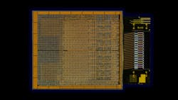
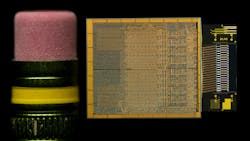
Intel’s Integrated Photonics Solutions (IPS) Group made a big splash at the Optical Fiber Communication Conference (OFC) 2024 with its fully integrated optical compute interconnect (OCI) chiplet. It was co-packaged with an Intel CPU to demonstrate the possibilities of integrating optical connectivity within the package for chip-to-chip interconnects (see figure).
One of the major challenges in high-performance computing (HPC) is connectivity bandwidth. Currently, data needs to be moved off-chip to optical interfaces to provide high-speed transfers and the longer distances provided by optical interconnects. Data centers and cloud computing are pushing the bandwidth requirements, but moving the optical connection within a chip package offers significant benefits: reduced footprint, increased throughput, and lower power requirements.
Artificial-intelligence and machine-learning (AI/ML) large language models (LLMs) represent just one application area that require this level of throughput. Military and avionics applications, such as phased-array radar, also mix HPC with lots of data.
What the System Looks Like
Intel’s chiplet incorporates 64 bidirectional channels running at 32 Gb/s for a total bandwidth of 4 Tb/s. The chiplet uses a hybrid laser-on-wafer technology and direct integration. And the overall system leverages eight fiber pairs, where each pair carries eight dense-wavelength-division-multiplexing (DWDM) wavelengths.
The OCI transmitters can drive up to 100 meters of fiber-optic cable. This is handy for off-board/off-system connections, but shorter on-board connections are useful as well because of high throughput and lower power requirements. The connection protocol is compatible with Peripheral Component Interconnect Express (PCIe) Gen5.
The 32-Gb/s transmit eye diagram illustrates high signal quality using single-mode fiber (SMF) patch cord. The co-packaged chiplet requires just 5 picojoules (pJ) per bit compared to an off-chip solution like a pluggable optical transceiver module, which typically requires 3X the energy or 15 pJ/bit.
The chiplet isn’t Intel’s first work with a silicon photonics integrated circuit (PIC). It has shipped over 8 million PICs with over 32 million integrated on-chip lasers—with a laser failures-in-time (FIT) rate of less than 0.1.
Why Put OCI On a Chiplet?
Intel’s demonstration pairs the chiplet with a CPU chiplet. However, providing a chiplet-based solution enables a chiplet-based solution to incorporate any mix of chiplets, such as GPUs, IPUs, or AI/ML accelerators. Universal Chiplet Interconnect Express (UCIe) is a standard chiplet interface that makes it easier to link chiplets together. Multi-vendor chiplet demonstrations have shown that the approach is practical.
Wide, high-speed interconnects within a chiplet-based platform can be facilitated by UCIe. Nonetheless, moving this level of interconnect off-chip usually requires significant interface chiplets that don’t have the same bandwidth as an OCI solution.
One reason for using chiplets is to split out functionality. Another is to provide different chip technologies within a single package. CPU, GPU, and AI/ML accelerators utilize different technologies versus the optical drivers and receivers used in this OCI.
Is an OCI Chiplet Just for Data Centers?
Data centers are able to easily utilize 4-Tb/s connections, but it’s not the only place where OCI can be beneficial. As mentioned, military and avionics applications often need this level of throughput to get data from sensors to the compute platform and then to distribute the results.
Many other embedded applications could benefit from high-speed, low-power connections provided by OCI, such as smart cars and medical applications with large amounts of sensor data. Processing this in real-time requires moving the data quickly and efficiently to the compute modules, e.g., AI/ML accelerators that are processing LLMs.
About the Author
William G. Wong
Senior Content Director - Electronic Design and Microwaves & RF
I am Editor of Electronic Design focusing on embedded, software, and systems. As Senior Content Director, I also manage Microwaves & RF and I work with a great team of editors to provide engineers, programmers, developers and technical managers with interesting and useful articles and videos on a regular basis. Check out our free newsletters to see the latest content.
You can send press releases for new products for possible coverage on the website. I am also interested in receiving contributed articles for publishing on our website. Use our template and send to me along with a signed release form.
Check out my blog, AltEmbedded on Electronic Design, as well as his latest articles on this site that are listed below.
You can visit my social media via these links:
- AltEmbedded on Electronic Design
- Bill Wong on Facebook
- @AltEmbedded on Twitter
- Bill Wong on LinkedIn
I earned a Bachelor of Electrical Engineering at the Georgia Institute of Technology and a Masters in Computer Science from Rutgers University. I still do a bit of programming using everything from C and C++ to Rust and Ada/SPARK. I do a bit of PHP programming for Drupal websites. I have posted a few Drupal modules.
I still get a hand on software and electronic hardware. Some of this can be found on our Kit Close-Up video series. You can also see me on many of our TechXchange Talk videos. I am interested in a range of projects from robotics to artificial intelligence.


