Co-packaged Optics Delivers High-Performance Chip Communication
What you’ll learn:
- Why co-packaged optics (CPO) are needed in high-performance computing (HPC).
- How IBM delivers CPO.
- What CPO means for HPC applications like artificial intelligence and machine learning.
Providing high-speed connections from one chip to another these days involves a host of electronics, including SerDes. Getting data from one compute engine to another or to storage requires the signals to move through these interface electronics, all of which add delay and consume power that generates heat.
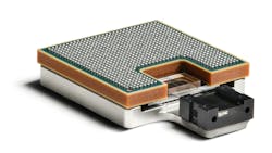
In many cases, optical connections are needed to go longer distances because copper connections, even running at 800 Gb/s, aren’t up to the task due to physics and physical constraints. Unfortunately, optical connections require additional buffering, which heretofore has been done with additional chips that have copper connections to the data source. IBM Research’s latest announcement on co-packaged optics (CPO) addresses this challenge (Fig. 1).
AI Acceleration Needs Co-packaged Optics Support
Before we dive into how CPO works, it’s worth explaining why this technology is so important. High-performance computing (HPC) and cloud computing have always pushed the limits of compute performance and connectivity. Optical-fiber cabling has been a requirement for the backbone to handle the growing speeds and connection distances.
Artificial intelligence and machine learning (AI/ML) in HPC environments have pushed bandwidth requirements significantly. Scaling systems with more optical transceiver chips pushes thermal-management limits, therefore any improvement would have substantial benefits to the scale and performance of a system.
Chiplet technology allows for optics to be added to a co-packaged solution. The trick is to enable direct optical connection to the optics chiplet, thereby removing additional external connections currently needed for standalone optical transceivers commonly in use today.
How IBM’s Co-packaged Optics Works
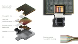
The optics are all about waveguides and coupling (Fig. 2). The chiplet with the optical drivers is below the waveguide, which routes the optical connection out of the chip via adiabatic coupling, where the waveguide is mated to single-mode glass fiber (SMF) array cables.
According to IBM’s Peter Hess, “The insertion loss of photonic integrated circuit (PIC) to SMF optical link has typically been 1.5 to 2 decibels (dB) per channel. But in this case, it has been demonstrated to below 1.2 dB per full optical link. In addition, demonstrations with 18.4-micrometer-pitch optical waveguides have shown less than 30 dB crosstalk, indicating this co-packaged optics technology is scalable to very high bandwidth density for chip interconnection.”
As with most optical systems, a single cable goes from point A to B. The reason for multiple fibers is to increase the bandwidth.
The cable connection is at the ferrule that’s part of the chip package. The cable connects one chip to another potentially on the same board, although with optical cables it’s possible to drive the data longer distances. Initially, packages having a single connection will be used in most instances, with a switch having multiple connections.
The other aspect of IBM’s CPO is the 6X increase in the number of fibers provided by the polymer optical waveguide (PWG). The PWG stacks up to four layers high, supporting up to 128 channels. This increase in beachfront density of 51 fibers/mm is accomplished by using smaller fibers with an 18-µm pitch, which exacerbates the design challenge for aligning the fiber cable with the chip’s optical waveguide. It does translate into an 80X improvement in overall bandwidth. Moving the optical drivers into the chip also reduces the latency and power requirements, leading to a 5X power reduction.
The system is compatible with existing component assembly processing standards. It passes the JEDEC reliability specifications at 50-µm pitch.
Not surprisingly, the drive for AI/ML and large language models (LLMs) is behind the demand for more bandwidth. To date, copper connectivity has handled much of LLM hardware support, such as NVIDIA’s NVLink. Copper may be able to hit 1.5 Tb/s, but distance will be limited.
About the Author
William G. Wong
Senior Content Director - Electronic Design and Microwaves & RF
I am Editor of Electronic Design focusing on embedded, software, and systems. As Senior Content Director, I also manage Microwaves & RF and I work with a great team of editors to provide engineers, programmers, developers and technical managers with interesting and useful articles and videos on a regular basis. Check out our free newsletters to see the latest content.
You can send press releases for new products for possible coverage on the website. I am also interested in receiving contributed articles for publishing on our website. Use our template and send to me along with a signed release form.
Check out my blog, AltEmbedded on Electronic Design, as well as his latest articles on this site that are listed below.
You can visit my social media via these links:
- AltEmbedded on Electronic Design
- Bill Wong on Facebook
- @AltEmbedded on Twitter
- Bill Wong on LinkedIn
I earned a Bachelor of Electrical Engineering at the Georgia Institute of Technology and a Masters in Computer Science from Rutgers University. I still do a bit of programming using everything from C and C++ to Rust and Ada/SPARK. I do a bit of PHP programming for Drupal websites. I have posted a few Drupal modules.
I still get a hand on software and electronic hardware. Some of this can be found on our Kit Close-Up video series. You can also see me on many of our TechXchange Talk videos. I am interested in a range of projects from robotics to artificial intelligence.
Voice Your Opinion!
To join the conversation, and become an exclusive member of Electronic Design, create an account today!

Leaders relevant to this article:


