eGaN® FET-Silicon Power Shoot-Out Vol. 13, Part 2: Optimal PCB Layout
With the significant reduction in package parasitics provided by the eGaN FET, the package inductance is minimized and is no longer the major parasitic loss contributor. The high frequency loop inductance, controlled by PCB layout becomes the major contributor to loss, making layout of the eGaN FETs critical to high frequency performance[1]. To verify this, different layouts with similar common source inductance and different high frequency loop inductances are compared and methods to reduce loop inductance by PCB layout are proposed.
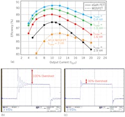
From the efficiency curves obtained from experimental prototypes, shown in Fig. 1a, the impact of layout on efficiency can be seen for the eGaN FET at 1 MHz. An increase in the high frequency loop inductance from around 0.4 nH to 2.9 nH results in additional loss, decreasing efficiency by over 4%. Another disadvantage of high frequency loop inductance is that voltage overshoot increases with loop inductance. Decreasing the high frequency loop inductance results in lower voltage overshoot, increased input voltage capability, and reduced EMI. Figs. 1band 1cshow the switching node waveforms for designs with a high frequency loop inductance of 1.6 nH and 0.4 nH; the voltage overshoot is reduced from 100% of the input voltage to 30%, respectively.
LATERAL POWER LOOP
The first conventional PCB layout places the input capacitors and devices on the same side of the PCB in close proximity to minimize the size of the high frequency loop [2]. The high frequency loop for this design is contained on the same side of the PCB and is considered a lateral power loop as a result of the power loop flowing on the board plane on a single layer. An eGaN FET design arranged in a lateral power loop was created and the part placement and high frequency power loop are shown in Fig. 2 with the high frequency loop highlighted in red.
Fig. 2.Conventional lateral power loop with eGaN FETs shown in (a) top view and (b) side view.
For this design, the inductor connection is made through internal layers using vias in between the top switch and synchronous rectifier. The driver is located in close proximity to the eGaN FETs to minimize common source inductance and keep the common source inductance constant between designs. This allows a comparison of only the influence of high frequency loop inductance.
While minimizing the physical size of the loop is important to reduce parasitic inductance, the design of the inner layers is also critical. For the lateral power loop design the first inner layer serves as a “shield layer” [3]. This layer has a critical role to shield the circuit from the fields generated by the high frequency power loop. The power loop generates a magnetic field that induces a current, opposite in direction to the power loop, inside the shield layer. The current in the shield layer generates a magnetic field to counteract the original power loop’s magnetic field. The end result is a cancellation of magnetic fields that translates into a reduction in parasitic inductance at the cost of increased eddy current losses within the shield. Having a complete shield plane in close proximity to the power loop provides the best performance.
For the lateral power loop design, the high frequency loop inductance should show little dependence on board thickness as the power loop is contained on the top layer. The lateral design should be very dependent on the distance from the power loop to the shield layer which is contained on the first inner layer [4]. To minimize loop inductance in the lateral power loop, the distance from the power loop and shield layer must be minimized.
VERTICAL POWER LOOP
Fig. 3. Conventional vertical power loop with eGaN FETs shown in (a) top view, (b) bottom view, and (c) side view.
The second conventional PCB layout places the input capacitors and devices on opposite sides of the PCB, with the capacitors generally being located directly underneath the devices to minimize the physical loop size (Fig. 3). This layout is considered a vertical power loop because the power loop travels perpendicular to the board plane with vias connecting the power loop vertically through the board. An eGaN FET design arranged in a vertical power loop was created, and the part placement and high frequency power loop are shown in Fig. 3 with the high frequency loop highlighted in red. Again, space is left between the devices to allow the inductor connection.
For the vertical power loop design, there is no shield layer due to the vertical structure of the power loop. As opposed to the use of a shield plane, the vertical power loop uses a self-cancellation method to reduce inductance. For the PCB layout, the board thickness is generally much thinner than the horizontal length of the traces on the top and bottom side of the board. As the thickness of the board decreases, the area of the loop shrinks significantly when compared to the lateral power loop, and the current flowing in opposing directions on the top and bottom layers begins to provide field self-cancellation, further reducing parasitic inductance.
In the vertical power loop design, the loop inductance is heavily dependent on the board thickness as the power loop is contained on the top and bottom layers of the PCB. Without the requirement of a shield layer, the distance between the first inner layer and the power loop has little impact on the inductance. To minimize loop inductance in the vertical power loop, the board thickness must be minimized.
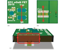
To enable the high switching speed available from the superior figure of merit (FOM), eGaN FETs were developed in advanced land grid array (LGA) packages that not only have low internal inductance, but enable users to design ultra-low inductance into their board. To provide the benefits of reduced loop size, magnetic field self-cancellation, consistent inductance independent of board thickness, a single sided PCB design, and high efficiency for a multi-layer structure, an improved layout is proposed for eGaN FETs. The design utilizes the first inner layer, shown in Fig. 4b, as a power loop return path. This return path is located directly underneath the top layer’s power loop, Fig. 4a, allowing for the smallest physical loop size combined with field self-cancellation. The side view (Fig. 4c) illustrates the concept of creating a low profile self-cancelling loop in a multilayer PCB structure. Table 1compares the characteristics of conventional and proposed optimal designs.
Fig. 4. Proposed optimal power loop with eGaN FETs, shown in (a) top view (b) top view of inner layer one, and (c) side view.
The improved layout places the input capacitors in close proximity to the top device, with the positive input voltage terminals located next to the drain connections of the top eGaN FET. The eGaN FETs are located in the same positions as the lateral and vertical power loop cases. Located between the two eGaN FETs is a series of interleaved switching node and ground vias arranged to match the LGA fingers of the synchronous rectifier eGaN FET. The interleaved switching node and ground vias are duplicated on the bottom side of the synchronous rectifier. These interleaved vias provide three advantages:
1) The via set located in between the two eGaN FETs provides a reduced length high frequency loop inductance path leading to lower parasitic inductance.
2) The via set located beneath the synchronous rectifier eGaN FET provides additional vias for reduced resistance during the synchronous rectifier eGaN FET freewheeling period, reducing conduction losses.
3) The interleaving of the via sets with current flowing in opposing direction allows for reduced eddy and proximity effects, reducing AC conduction losses.
EXPERIMENTAL RESULTS
To compare the performance of the proposed optimal power loop with conventional lateral and vertical designs for a wide range of applications, four separate board builds were created. The designs varied the overall thickness of the board and the distance between the top layer and the first inner layer in the board (inner layer distance). The part layouts remained unchanged (shown in Figs. 2, 3,and 4), and all designs were comprised of four layers with two ounce copper thickness.
Fig. 5 (a) PCB cross section of board thickness showing Inner layer distance for experimental designs, and (b) Simulated high frequency loop inductance values for lateral, vertical and optimal power loops with different board thickness and inner layer distance.
The values of the high frequency loop inductance for varying board thicknesses and inner layer distance, defined in Fig. 5a, were simulated and the results are presented in Fig. 5b. From the data it can be seen that for the lateral power loop the board thickness has little impact on the high frequency loop inductance while the inner layer distance significantly impacts the inductance. For the vertical power loop, the inner layer distance has very little impact on the inductance of the design, while the board thickness impacts the inductance by as much as 80% when the board thickness is doubled from 31 to 62 mils.
For the proposed optimal layout, the design shares the traits of the lateral power loop by showing little dependence on board thickness and a strong dependence on inner layer distance. This design provides a significant reduction in loop inductance from the removal of the shield layer and reduced physical size of the power loop; traits similar to the vertical power loop design. Combining the strengths of both conventional designs, the proposed design can reduce inductance up to 65%, compared to the best conventional lateral or vertical power loop.
Fig. 6. Experimental loss plot for lateral, vertical and optimal power loop designs
VIN=12 V, VOUT=1.2 V, IOUT=20A, FSW=1 MHz, LBUCK=300 nH.
Top switch is EPC2015, synchronous rectifier is EPC2015.
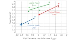
The power loss for the three different loop layouts, constructed with different board thicknesses and inner layer distances is shown in Fig. 6. From this data it can be seen that for similar parasitic inductances the power loss of the lateral loop is higher than the vertical and optimal loop. The cause of the increased loss in the lateral power loop can be attributed to the additional loss in the shield layer, which is not required in the vertical or proposed optimal power loop. The experimental hardware verifies the trend of increased loop inductance and higher power loss.
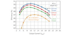
Fig. 7. Efficiency comparisons for different loop designs with VIN=12 V, VOUT=1.2 V, FSW=1 MHz, LBUCK=300 nH, board thickness=31 mils, and inner layer distance=4 mils. The eGaN FETs are top switch EPC2015, synchronous rectifier EPC2015. MOSFETs are top switch BSZ097N04LSG, synchronous rectifier BSZ040N04LSG.
Fig. 7shows the efficiency results of the three proposed designs compared to a silicon implementation utilizing a vertical power loop with the smallest commercial package, a 3 x 3 mm TSDSON-8, to minimize the power loop. For the Si MOSFET design, the high frequency loop inductance was measured to be around 2 nH, compared to 1 nH for a similar power loop using eGaN FETs. This is due to the large packaging inductance of the Si MOSFET dominating the loop design. As a result of the superior FOM and packaging of the eGaN FETs, all of the power loop structures outperform the Si MOSFET benchmark design. The optimal power loop produces a 3% full load efficiency improvement for the eGaN FETs, as compared with the Si MOSFET benchmark design.
For the different eGaN FET designs, the optimal power loop provides a 0.8% and 1% full load efficiency improvement over the vertical and lateral power loops, respectively. For all of the design tests, the optimal layout provides the highest efficiency and lowest device voltage overshoot.
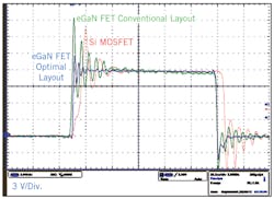
Fig. 8. Switching node waveforms of optional eGaN FET, conventional eGaN FET, and MOSFET designs at VIN=12 V, VOUT=1.2 V, IOUT=20A, FSW=1 MHz, LBUCK=300 nH. The 40 V eGaN FETs are top switch EPC2015, synchronous rectifier EPC2015; MOSFETs are top switch BSZ097N04LSG, synchronous rectifier BSZ040N04LSG.
Fig. 8shows the switching waveforms for the eGaN FET conventional and optimal layouts and Si MOSFET benchmark. Both eGaN FET designs offer significant switching speed gains compared to the Si MOSFET benchmark. The eGaN FET with the conventional vertical layout suffers from a large voltage spike at high switching speed. An optimal layout eGaN FET design offers a 500% increase in switching speed with a 40% reduction in voltage overshoot compared to the 40 V Si MOSFET benchmark. For the eGaN FET with low package parasitic inductance, the layout is critical to high- speed switching and limiting device overshoot.
With the reduced overshoot achieved by the optimal eGaN FET layout, the converter handles higher input voltages with low voltage rated devices. The converter was operated at inputs of 12 V, 19 V, 24 V, and 28 V, and the efficiency curves are shown in Fig. 9. Due to the voltage overshoot in the MOSFET design, its operation was limited to 12 V, 19 V, and 24 V.
Fig. 9. eGaN FET optimal layout and MOSFETs at varying input voltages showing efficiency comparison, and switching waveforms: VIN=24 V, VOUT=1.2 V, IOUT=20A, FSW=1 MHz, LBUCK=300 nH. eGaN FETs are top switch EPC2015, synchronous rectifier EPC2015. MOSFETs are top Switch BSZ097N04LSG, synchronous rectifier BSZ040N04LSG.
The introduction of high performance eGaN FETs offers the potential to switch at higher frequencies and efficiency than possible with traditional Si MOSFETs. Combined with improved FOM and low parasitic packaging, eGaN FETs enable extremely low high frequency loop inductance layout to fully utilize the device’s capability. Using an optimal layout approach further enhances the benefits of eGaN FETs, providing additional efficiency gains and higher voltage operation.
REFERENCES
[1] D. Reusch, “eGaN-Silicon Power Shoot-Out Vol. 13, Part 1: Optimizing PCB Layout” Power Electronics Technology, March 2013.
[2] Application Report SLPA010 – “Ringing Reduction Techniques for NexFET High Performance MOSFETs,” November 2011.
[3] Michele Lim, “Low Temperature Co-fired Ceramics Technology for Power Magnetics Integration”, Ph.D. Dissertation, Virginia Tech, 2008.
[4] D. Reusch, J. Strydom, “Understanding the Effect of PCB Layout on Circuit Performance in a High Frequency Gallium Nitride Based Point of Load Converter,” APEC 2013. March 2013.
About the Author
Voice Your Opinion!
To join the conversation, and become an exclusive member of Electronic Design, create an account today!

Leaders relevant to this article:
