AI Engines Augment ACAP FPGA
Xilinx’s Adaptive Compute Acceleration Platform (ACAP) blends FPGA flexibility with hard-core logic that provides power-efficient acceleration. A high-speed, programmable, network-on-chip (NOC) connects everything together. The system has a 9-Tb/s serial interface bandwidth to move data in and out of the chip quickly. The chips also include ASIC-like cores such as 100G/600G Ethernet cores, 400G high-speed crypto engines, and DDR memory control.
The latest addition to the ACAP portfolio is the Versal Premium Series with AI Engines (Fig. 1). This 7-nm family adds artificial-intelligence (AI) engines to the DSP engines that were already included on prior ACAP chips.
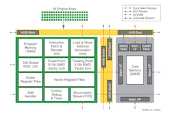
The main building block of these AI ACAP chips is the AI Engine tile (Fig. 2). The blocks contain dedicated instruction and data memory—16 kB and 32 kB, respectively. This supports a 32-bit scalar processing unit that can handle 512-bit fixed-point and 512-bit floating-point vector processing with their own vector register sets. The memory units and computational units are linked to their nearest neighbors within the array of AI Engine blocks. The NOC connects the AI Engine array with the rest of the units on the chip.
A typical application for the AI ACAP chips is radar processing that employs machine-learning (ML) models in the data-stream processing flow (Fig. 3). The system is designed to deliver twice the beamforming performance in a smaller footprint using half the power of a more conventional approach.
About the Author
William G. Wong
Senior Content Director - Electronic Design and Microwaves & RF
I am Editor of Electronic Design focusing on embedded, software, and systems. As Senior Content Director, I also manage Microwaves & RF and I work with a great team of editors to provide engineers, programmers, developers and technical managers with interesting and useful articles and videos on a regular basis. Check out our free newsletters to see the latest content.
You can send press releases for new products for possible coverage on the website. I am also interested in receiving contributed articles for publishing on our website. Use our template and send to me along with a signed release form.
Check out my blog, AltEmbedded on Electronic Design, as well as his latest articles on this site that are listed below.
You can visit my social media via these links:
- AltEmbedded on Electronic Design
- Bill Wong on Facebook
- @AltEmbedded on Twitter
- Bill Wong on LinkedIn
I earned a Bachelor of Electrical Engineering at the Georgia Institute of Technology and a Masters in Computer Science from Rutgers University. I still do a bit of programming using everything from C and C++ to Rust and Ada/SPARK. I do a bit of PHP programming for Drupal websites. I have posted a few Drupal modules.
I still get a hand on software and electronic hardware. Some of this can be found on our Kit Close-Up video series. You can also see me on many of our TechXchange Talk videos. I am interested in a range of projects from robotics to artificial intelligence.


