This file type includes high resolution graphics and schematics when applicable.
In the development of SoC-based (system-on-chip) circuit boards, the SoC’s additional capabilities will provide abundant functional benefits. But at the same time, these capabilities can introduce additional challenges to the circuit board manufacturing process. Therefore, developing an effective plan for designing, developing, testing, and producing the final printed-circuit boards (PCBs) is good business practice.
Several steps in the PCB development process include areas that allow enhancements that can improve the ease of board manufacturing and the yield rate of the production circuit boards. Many elements of the process, from the SoC itself to the design process to the end board tests, should be reviewed for improvements that can affect the PCB’s final manufacturability.
Size Does Matter
SoC devices have a certain inherent complex nature. An entire system is packed into a single silicon package the size of your thumbnail. There are many interfaces, clocks, signals, protocols, and power connections within a small physical structure. The reduction in the size of the system does not guarantee a reduction in PCB implementation issues. In some cases, this physical reduction increases the number of challenges that will be encountered when designing the underlying PCB.
To fit so many combinations of function within the same small package, the chip’s designers usually use a clever method of assigning multiple combinations of function to the same pin. On the Texas Instruments (TI) Sitara AM3358 processor, for example, the same pin can be assigned UART, I2C, general-purpose I/O (GPIO), Reduced Gigabit Media Independent Interface (RGMII) Ethernet, or motor drive pulse-width modulation (PWM) functions, representing only a few of the available interfaces.1
Related Articles
- The Engineer's Guide To High-Quality PCB Design
- PCB Design And Its Impact On Device Reliability
- Low-Power Analog Interface Circuit Design Techniques For SoCs
This use of temporal assignment of multiple interfaces on the same physical structure, the I/O cell, is a great way of developing a low-cost system solution. In many ways this can help reduce the overall system cost and take advantage of ever-shrinking silicon processes. Using I/O pin multiplexing like this can present some challenges at the PCB level, though.
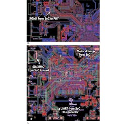
Implementing a system using an SoC with a complex I/O pin multiplexing scheme presents a challenge in that the same PCB layout is not optimal for all the possible I/O pin definition combinations. Figure 1 shows the PCB layout for two different I/O selections from the same SoC. In circuit design A, a set of pins is configured for a UART, an SD/MMC card, GPIO, and motor control. In circuit design B, the same set of pins is configured for an Ethernet bus using the RGMII type of interface.
Note that at a schematic level, there does not seem to be much difficulty changing between the two designs since it’s simply replacing the end devices/circuits with the appropriate choices (such as an RS-232 transceiver versus the Ethernet physical layer, or PHY). However, when the PCB layout implementation is reviewed, a dramatic change in the requirements for the different interfaces reveals what major changes must be made to the PCB placement and subsequent routing to develop a robust circuit board. The UART, SD/MMC card, GPIO, and motor control will be routed to multiple devices that may be placed at spatially diverse positions on the PCB. In contrast, the Ethernet bus will be routed to a single device, the Ethernet PHY, which will probably be placed fairly close to the SoC.
This difference in the routing of the same SoC pins depending on the interface connection reveals why there is not a single global correct way to lay out an SoC-based PCB that works for all designs. Instead, each design needs attention to such details to minimize the risk of manufacturability issues. Reference designs from the SoC manufacturer can help show pragmatic implementations of common circuit designs.
Planning Ahead
By the time the first PCBs arrive, many design issues can be checked. The process of designing the PCB in an efficient way has much to do with what items can be verified early in the design. The steps in the process can help move the high-risk items earlier in the process to give you more time to recover from possible errors in the design or implementation. However, some of the PCB design process must be carefully thought out to meet the pre-requisites of each step (Fig. 2).
In a common PCB build environment, the main goal, of course, is to use the schematic design to build a tangible real PCB. Several different materials can be used to generate the circuit board. For this discussion, rigid FR-4 material is assumed to be used. The intricate physical and material characteristics of the FR-4 copper-clad glass epoxy board are beyond the scope of this article. However, these very details of the PCB material can contribute to important design decisions, starting with the requirements of the board all the way through testing and production manufacturing. As a part of the PCB requirements and design steps, it helps to understand these details because details such as copper weight and board stock insulation thickness will determine the stackup and steer the routing constraints for the board.
In some instances, it may seem easy to leave the board physical parameters to the layout person. But maintaining even a cursory knowledge of the underlying board substrate can allow better decisions that affect many items going back to certain characteristics such as how big the board can be and what devices can be placed on the PCB.
For example, FR4 material has a certain amount of flexibility across its lateral and longitudinal dimensions. If this is not addressed, then a ball grid array (BGA) the size of an SoC could result in solder ball bond failure if unforeseen mechanical stress is placed on the board. In a different way, mounting the PCB can add to issues of thermal failure and board twist/mechanical flexing depending on the enclosure/rack assembly.
Though at first view of the PCB design process, the end production board is the key metric to be seen, the use of and actual need for early prototype circuit boards is an important step in the overall PCB flow. Despite a careful view of the design activity and checklists that verify that design constraints have been met, errors in the design can slip through and show up in the final board. Therefore, early prototype boards are important for flushing out errors and misjudgments in a SoC board design.
What errors can happen when there has been due diligence during the design of a circuit board? Several things can go wrong with even the best-intentioned SoC-based circuit board design:
- Communication mistakes between the board designer, requirements team, layout person, or board manufacturing partner
- Too large a scope of the design leaving unhandled requirements
- Component footprint errors
- Mechanical placement errors (connector/cable clearance issues, display mounting problems, etc.)
- Misunderstanding of the board requirements
- Electrical design mistakes
- Power supply problems
- Interface signal noise problems
- Orientation of device/daughterboard connectors
- Error in the address assignment of devices
- Board configuration option functional issues
- Component availability problems
- Component revision changes by the manufacturer
Establishing Goals
Simulation technology has improved noticeably in recent years, and tools employing it can be used to try to catch some of these types of problems. While a large effort to simulate the design, verify mechanical clearance, confirm design requirements, and think through how configuration options can minimize potential errors (and all these activities are good design practices), the increase of the design schedule to accomplish all of these steps realistically can be more than the board development constraints will allow.
It is very important to drive to clear and succinct design goals as an early part of the PCB design process. These design goals can seem general and nebulous before expounding on them during the design phase. Goals that are left vague leave an opportunity for misunderstanding, which will manifest as PCB faults that can affect the straightforward build schedule of the final PCBs.
For instance, if a particular NAND flash memory must be used, but the I/O voltage level is not clear, then the circuit may be designed for supporting both 1.8 V and 3.3 V or it may be designed for a single voltage value. For seamless connection to the SoC, this I/O voltage level must be matched on the corresponding supply rail on the SoC. This can add unneeded complexity and risk to the board. When there is any doubt about requirements, reviews can clarify these questions.
Component placement upon the circuit board has huge effects on the manufacturability of the final PCB. The optimal placement of the components affects inter-device clearance, manufacturing pick and place efficiency, cable access and clearance, and soldering profile differences. This is different than the I/O multiplexing issues explained earlier, although they are often related.
Issues such as lead versus lead-free components placed next to each other can make it more difficult to set the proper soldering profile for the board. (This is less of a problem now with improvements in soldering technology.) Typically, lead-free components require a higher solder such as 250°C while lead components may require 220°C.2 Placing these components right next to each other could affect manufacturability due to differential thermal convection. This is especially true for ultra-small BGA components (such as single gates in discrete packages) that have only a few balls for attachment and lower thermal mass.
If one particular component has rigid routing constraints, this may limit the placement of other components within a certain region. For instance, high-speed interfaces such as DDR3 require constant reference planes and effective isolation from other interfaces. This will limit placement of other devices within a certain distance of the DDR3 memory devices.
In a SoC type of design, many heterogeneous peripheral devices often must function on the same PCB. Preparing a priority-based placement analysis can help ensure a proper functioning final circuit board. Floor-planning the PCB prior to component placement helps to reveal potential routing, power, and mechanical problems.
Usually a circuit board has certain physical constraints for connector placement based on the planned uses of the PCB and the end product that it is in. Sometimes the SoC has multiple sets of I/O to which a particular interface can be mapped. Using a floor plan of the PCB can reveal better combinations of I/O mapping of the SoC pins that will provide better mechanical structures on the circuit board.
On The Board
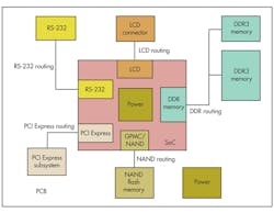
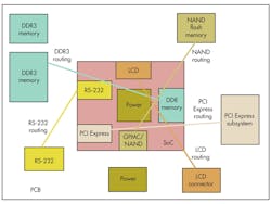
The placement in Figure 3 will clearly provide a better board that is easier to lay out and build than the other board. The floor plan has the devices spatially optimal for routing since the locations of the appropriate SoC balls for each interface are oriented near the position of the external device on the board. Figure 4 illustrates a floor plan that has the components placed away from the corresponding interface balls on the SoC processor. This will require routing lanes that cross each other and consume valuable board power and signal routing area. Remember, there are only so many layers to route signals and power and cost increases to gain more layers for routing.
While this may seem obvious when looking at the design at this level, sometimes other board requirements such as connector placement will force non-optimal placements to occur. Looking at the floor plan of the board can show issues that may not be intuitive when considering only the electrical connections of the schematic.
As a general rule in an SoC-based design, escaping the SoC’s ball array is of primary concern, not just for signals but also for power and ground connections. If a low-cost PCB is an important constraint, then there are limitations to how the signals can be routed from all the balls on the SoC package. For instance, in a 15- by 15- by 0.8-mm package with most of the ball array populated, routing escape can be more difficult if the supporting components are placed in poor locations or at distances from the SoC that are not conducive to the planned board size.
Splitting the design into multiple boards for whatever reason can increase the complexity. If the board constraints require multiple boards, extra planning and verification are necessary to maintain signal integrity on critical interfaces as well as to ensure mechanical clearances are correct.
This is another example of using early prototypes to bolster the spatial component analysis and verify that there will not be production problems. The introduction of the second (or additional) boards to the physical construction adds another dimension where components may interfere with each other where they wouldn’t on a single PCB solution.
Preparing For Contingencies
As foolproof as modern components have gotten, it is still important to investigate the planned components for a PCB design to help minimize impact to the end board build. Some components have less than apparent packaging details. While standard packages exist for many ICs and discrete components, some packages have peculiar attributes that make them susceptible to soldering errors and other assembly errors such as non-standard pin pad geometries or assignments.
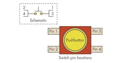
For instance, in Figure 5, the momentary pushbutton switch would appear at first glance to have pins 1 and 2 shorted together and 3 and 4 shorted together based on the proximity of each pair of pins. But the device schematic from the datasheet indicates that the other sets of pins are actually connected.
Using components with these types of irregularities introduces more risk into the overall PCB design flow. While the irregularity can be compensated for, it is easy to miss these details when there are so many other details to verify and check prior to pattern generation for PCB fabrication.
A major concern for manufacturability of a board rests with the component selection. As hardware board designers, we usually concentrate on the board details. But the simple details about the components such as the product lifetime of the chosen components for the design can spell disaster for a board build schedule if the availability of the chosen devices is a problem.
A worse case is if the component is no longer available with no alternative device or second sources available. The PCB then usually must be redesigned to accommodate a replacement component. Added to this redesign is the obvious concern about checking whether the new component will cause any new problems that had already been answered for the old component. An SoC-based design may have additional requirements if there is a close coupling of the SoC to some external devices.
As discussed earlier, the PCB material can also have major implications for the manufacturability of a SoC-based design. The construction of the PCB itself will be dictated by some of the overall design requirements such as cost, size, board outline, and more. Normal board constraints call for “smaller is better” when it relates to overall PCB physical size. Smaller physical size decreases the amount of space for routing traces and placing components. When considering solutions to placement and routing issues caused by any reason, simple changes such as just adding more layers to the PCB might at first seem attractive but may not be the correct answer.
Consider a 120- by 95-mm PCB with a central SoC processor that is in a 17- by 17-mm package with a 625-ball array in a 0.65-mm pitch. There will be other devices on the board, and some of them may be BGA-type packages. The major challenge in proper layout of the PCB will be the routing escape from the SoC. Depending on the number of signals actually used on the SoC for the design, routing each SoC pin to the target on the PCB may be challenging.
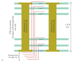
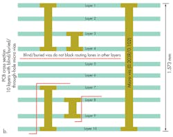
While the signals are one aspect to the routing job, the power distribution network (PDN) is just as important. In today’s modern SoC processors, the power delivery is very important to minimize erratic runtime failures, which are difficult to diagnose. This is where one solution does not work for all implementations. If cost and schedule were no issue, then a common solution would be just to increase the layer count and use more complex and smaller via types (Fig. 6).
This approach effectively compensates for the reduction in gross spatially X&Y routable area and volume (remember, routing is in 3D) when the overall board size is shrunk by reducing the physical volume of the signal and power vertical transition zones (vias) and increasing the routable Z-axis area. The downside to this is that each additional layer pair added increases the PCB cost and time.
Furthermore, the use of anything other than through-hole vias of a particular diameter and pad size will increase the fabrication steps due to the requirement to drill before fabrication adhesion of outer layers. Also, using non-mechanical drills due to the small diameter via physical size will increase the PCB fabrication cost. The industry has improved much in this area over the last decade, but 12-layer boards with micro-vias and blind/buried vias are still not equal in cost with four- or six-layer boards with through-hole vias only.
Testing And The Big Picture
Each design should be evaluated separately to determine the optimal solution. For instance, the SoC will typically have a massive amount of routing running to it, and it will also demand a decent amount of power network planes, partial planes, or wide traces. Adding layers will generally help in routing escape from the SoC, but the additional cost of the PCB with the extra layers may not be tolerated from an end-cost point of view.
It’s important to specify and track the specific placement and signal design constraints for the board. The very process of specifying these constraints may flush out some competing requirements that can be resolved early on. At the very least, these constraints help to guide layout from a more proactive stance in a group-type organization. This really helps to show the critical signals such as DDR3, MIPI, Ethernet RGMII, and more, as well as how these signals need to be prioritized during placement and layout to improve their traces’ signal integrity.
After all, due to certain signal integrity requirements of some interfaces, a PCB physical area will have certain prime routing locations that command short distance between specific components, great reference plane locations, and faster wavefront flight times due to layer characteristics. By targeting the critical nets to occupy these prime routing locations, the resulting PCB has a lower risk of board failure due to crosstalk issues, power supply noise issues, component tolerance problems, and beyond.
Even if a design is proven to function within specification, there is no guarantee that each production unit will function within that specification. Due to the many variables associated with building a modern SoC-based circuit board, items such as component tolerance, soldering mishaps, assembly errors, PCB fabrication mistakes, layout problems, and plain human error can cause yield problems in production PCBs.
Therefore, a proper board development process that seeks high yield of final circuit boards should include some type of diagnostic testing. These tests should be run on every single production board before it is packed and shipped. SoC processor-type boards include multiple heterogeneous interfaces that all have specific functional requirements. Therefore, the diagnostic tests should include a test or series of tests for each of these interfaces. Knowing and clearly defining the requirements of the board pays big benefits here by making it easy to understand, define, and write the tests that are necessary to qualify a board for pass/no-pass status at manufacturing time.
Usually the steps to developing these diagnostic tests include:
- Defining the important interfaces/power that need to be functionally tested
- Prioritizing these tests based on circuit requirements.
- Deciding on test coverage required for each test.
- Developing the tests.
- Checking the tests on a prototype board.
- Generating the optimized run version of the diagnostic tests.
Test yield coverage can be tuned based on the known requirements and perceived risks for a particular board. Typically, 100% test coverage of the hardware board is not fiscally feasible due to the board diagnostic test development costs and run-time costs incurred at production time. Thus, if the design has been proven to work, seeking full hardware test coverage is not necessary at production testing due to lower inherent risk of the design.
It is best not to have the same software developers who will develop the board SoC production software also write the diagnostic tests. At first this seems counterproductive. Since the software developers know the hardware from their work, surely this will save time and resources by using them to write the hardware board diagnostic tests. However, in reality the opposite is true.
The software designers who are very familiar with the hardware can sometimes be blinded into using the same software implementations that work in production software/firmware and placing it in the diagnostic test code. The point of the diagnostic tests is to flush out potential hardware problems. Therefore, having these tests written by someone other than the normal software development team will allow the test software to control the hardware in different ways that can and do show potential problems even before the production software is loaded and run.
This is another area where having early prototype boards is very important since they can be used for early diagnostic test development, which in turn improves the hardware design since the early tests can flush out early errors in the hardware design or incorrect implementations of the board requirements. The early prototype boards also give the diagnostic tests an additional benefit of being troubleshooting guides for the software team when they finally receive fully functional and tested circuit boards since they can refer to these tests if they run into problems during their development.
The tests are typically written with no operating system to make sure they have fewer dependencies and provide simpler hardware management techniques. The final step to the diagnostic test development is to optimize the tests into runtime executable code that can be run on each production board.
It is crucial not to skip this step since the per-unit test time should be minimized for production boards since each second of test time costs a certain amount. Nonetheless, diagnostic testing is worth the cost of development and execution because it improves board yield. Also, overall board manufacturability is improved since important test time data about the design can be observed and sent to the board designer for updates to the next version of the board.
Conclusion
As can be seen from these examples, several steps in the PCB development process will have more impact on the manufacturability of the PCB. Having the knowledge of these issues and developing a process for minimizing their potential impact can go a long way toward increasing the manufacturability of a circuit board during the design phase of the project.
This file type includes high resolution graphics and schematics when applicable.
References
Texas Instruments AM335x8 datasheet: http://www.ti.com/lit/ds/sprs717f/sprs717f.pdf
JEDEC Standard J-STD-020D.1
