Low-Power Analog Interface Circuit Design Techniques For SoCs

This file type includes high resolution graphics and schematics when applicable.
The quest for power reduction in electronic circuits is one of the main drivers of circuit design innovation. Recently, the need to reduce power consumption has extended beyond the territory of battery-powered applications such as handheld devices and remote sensors to plug-in applications such as home entertainment to meet green label requirements and even cloud storage and processing due to the sheer amount of power used in these compute farms (Fig. 1).

Related Articles
- Reduce Power In Computing And Memory Interfaces Without Impacting Performance
- Design Custom Chips That Maximize Battery Life
- Manhattan And Mr. Spock Offer Lessons In 3D FinFET Design
Furthermore, the use of ever more advanced process nodes, as described by Moore’s Law, leads to chips with higher functionality (gate density) in the same area. As a result, more power per area unit is generated inside the chip, despite the lower supply voltage. This excessive power is problematic unless it is properly dissipated, which requires expensive packages or heatsinks. The higher functionality of today’s systems-on-chip (SoCs) is driving the integration in the SoC of the analog interfaces with the multitude of signal sources that exist in modern devices, such as the output of wireless radios, wireline transceivers, and sensors.
Reducing Power
Power consumption can be reduced in multiple ways. In the digital domain, power supply levels often are reduced in line with the evolution of technology. The well-known formula for dynamic power dissipation (P) shows quadratic gains when supply levels (Vdd) are reduced:

Additionally, this formula highlights other strategies that yield immediate gains in terms of power dissipation: reduce the capacitance (C) being toggled (typically comprising gate capacitance plus any additional routing parasitic) and reduce the activity (a) of the circuit, through clocking strategies and, eventually, clock gating. The toggling rate (fclk) can also be reduced in some cases, although it would have the unintended effect of reducing processing speed.
However, the analog interfaces are in the analog domain where static power components typically dominate power dissipation, limiting the potential gains that can be achieved through the equation above. Furthermore, analog performance requirements, especially linearity and noise, often limit the ability to reduce the supply levels and demand the use of power-hungry high-gain circuits.
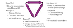
In traditional analog circuits, power must be traded off for speed (bandwidth) and/or resolution (linearity), for example (Fig. 2). Based on these tradeoffs, one could conclude that high-performance analog blocks cannot offer low power consumption, and therefore limit the overall system power. All is not lost, though. This conclusion is, contradicted by the sheer amount of scientific and development work dedicated to the subject of low-power analog circuit techniques.
Many pure analog circuits have been implemented to save power and allow for low-supply-voltage operation by using techniques such as sub-threshold operation (a region below the transistors’ normal operating region). These established techniques are effective in low-speed, medium-performance applications such as remote sensors and wristwatches.
For applications with higher speed or performance requirements, designers can take advantage of the abundance of digital transistors available in any modern process to significantly reduce the power (and area) of analog blocks at the expense of a (typically) modest area and power increase for the digital block.
For example, designers can minimize the tradeoffs between performance and power dissipation by transferring some of the complexity and performance requirements from the analog domain to the digital domain. This can be achieved by relying on techniques such as digital compensation, digital calibration, and higher digital processing speed, leading to digitally enabled analog circuits.
Such techniques allow designs to attain high levels of accuracy with lower power dissipation. They are directly applicable to circuits that rely on matching, such as pipeline analog-to-digital converters (ADCs) and successive-approximation register (SAR) ADCs. They rely on digital calibration algorithms that are embedded in the same circuit, which can analyze the “errors” and compensate for them autonomously, at power-up or during normal operation. By running this background calibration, the circuit also benefits from corrections to potential temperature or voltage drifts.
Multiple Situations
Digital calibration and compensation techniques can be used in a wide variety of situations in analog interface circuits such as ADCs:
• Offset compensation: Circuit mismatches make offset unavoidable in analog circuits. The simplest way to improve matching is to increase the size of all devices, which directly penalizes power dissipation and area. Alternatively, measuring it can compensate for the offset—for example, by comparing the output voltage to 0 and then balancing the circuit by adding some adjustment voltage through a small digital-to-analog converter (DAC).
• Gain error compensation: Low gain accuracy across the operating range of an amplifier can adversely affect linearity. Closed loop gain requires high open loop gain, which is typically achieved at the expense of power dissipation. Gain calibration can compensate for gain inaccuracy, without requiring high open loop gain. It is achieved by injecting a small-scale signal (typically at noise level) that can be measured through correlation and then subtracted. Highest correlation is achieved when the gain is compensated. The algorithm’s task is to find the coefficients that maximize the measured correlation.
• Mismatch between devices: Switched capacitor circuits such as ADCs rely heavily on the matching of capacitors to guarantee their accuracy. Relative matching is a function of device area. Capacitor matching errors can be calibrated by observing that the nominal value of each capacitor is equal to the sum of the remaining lower-order capacitors in the array. This comes naturally from the binary weighted nature of the capacitor array. The total capacitance is only dictated by the noise constraint, reducing the power spent in switching a large capacitor.
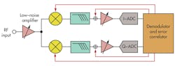
Digital calibration and compensation techniques are not confined to the analog block level. By taking advantage of the fact that the analog block is embedded in a complete system, including all of the digital signal processing stages, the system can estimate the quality of the signal being processed across the complete signal chain. It can then determine the required adjustment parameters for the analog blocks across the complete analog signal processing chain. These techniques are very efficient for compensating for mismatches, phase deviations, and distortions (Fig. 3).
Overall, these circuit techniques relax the performance requirements of the analog blocks, which can minimize both power consumption and area. They are particularly effective when the circuit is implemented in advanced process nodes and can take full advantage of the benefits of scaling.
In addition to the techniques that improve on established architectures, the analog blocks’ power dissipation can be further reduced with simpler architectures while maintaining performance objectives. For example, when compared to a pipeline architecture, a SAR-based architecture is much simpler and does not rely on multiple stages (each containing large gain amplifiers) to achieve performance goals. Rather, the SAR-based architecture is a single-stage comparator, which is inherently very compact and low-power. The beauty of this architecture is that no power-hungry precision amplifier is required, as it employs only blocks that can be designed with no static consumption.
The drawback of SAR-based architectures is their limited speed. However, this limitation is overcome in advanced process nodes by taking advantage of the high speed of the process as well as the high processing power available to implement digital assisted algorithms that allow further power reduction.
Conclusion
Power consumption reduction is an overwhelming requirement for integrated electronic circuits. As digital scaling requirements and the semiconductor technology roadmap push ICs to more advanced nodes, the analog blocks follow the same power reduction paradigm as the digital blocks in the same circuit, but not necessarily in the same manner. The move to smaller technologies encourages innovation in analog interface circuit design techniques that enable aggressive power and area reductions.
For more information, visit www.synopsys.com/IP/AnalogIP/DataConversion.

About the Author
Manuel Mota
Senior Manager, Product Management, Die-to-Die IP, Synopsys
Manuel Mota is currently Senior Manager of Product Management for Die-to-Die IP at Synopsys. He holds a Ph.D in electronic engineering from Lisbon Technical University and has held research and technical positions at The European Organization for Nuclear Research (CERN) in Geneva, Chipidea, and MIPS.
Comment About the Article
To join the conversation, and become an exclusive member of Electronic Design, create an account today!

Leaders relevant to this article: