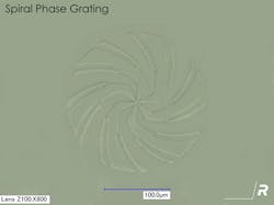
Rambus is developing a tiny lensless imaging system that covers a typical photodiode array with a specially designed diffraction grating. The diffraction approach eliminates the lens and support structure used with a refraction-based camera, but the data does require significantly more preprocessing to obtain an image (Fig. 1). Luckily, this can be done using a conventional DSP or GPU.
Figure 1. The lensless imaging system uses a specially designed spiral diffraction grating above a photodiode array.
Related Articles
- PoE/USB3 Camera Controllers Enrich Machine Vision
- Dual Camera Module Focuses Images After Taking Photos
The diffraction-based imaging system trades off mechanical complexity and cost for computational complexity. At this point there is a resolution limitation. The current sensor provides a 128- by 128-pixel image with a 100-degree view. The resolution is not likely to grow significantly, and telephoto operation is not applicable because there is no lens involved.
Download this article in .PDF format
This file type includes high resolution graphics and schematics when applicable.
Part of this limitation is also based on the diffraction approach as well as the diffraction grating. In particular, the diffraction grating needs to work with the range of visible light. Still, many insects and other animals function with this level of resolution. Similarly, many proximity-sensing applications can operate without high-resolution images.
Essentially the system uses the diffraction grating to spread incoming light across the sensor array. This means that light from a source will hit multiple pixels. The software then extracts the image by reducing the complex mapping imposed by the diffraction grating. The spiral architecture then comes into play because the algorithms know about its structure so it can decompose the captured data into the original image.
Compare this to a refraction approach where the lens focuses light from a source onto adjacent pixel sensors. In this case it is a simple matter of dumping the sensor data to obtain the image. The advantage is the simple sensor implementation and minimal data-packing overhead compared to some complex calculations for the new diffraction approach. The lens-based system scales well but requires more expensive glass optics to deliver high-quality images.
The diffraction approach won’t be replacing the technology in digital cameras anytime soon, but it does have advantages that make it an ideal sensing technology, especially for systems designed for the Internet of Things (IoT). For example, tasks like motion sensing and basic object position sensing require quite a bit of computation to analyze an image. This would take more time with a diffraction system if the image was recreated first, but tasks like this are easier to accomplish using the raw data from the sensor array. Changes from a region being viewed will show up as changes in one or more pixels on the sensor array, so it is possible to have a “tripwire” of a few pixels instead of analyzing the whole image to detect the change. This significantly reduces processing requirements and, hence, power consumption.
The system also makes tracking of angular movement between images easier since it can track a fractional pixel movement because the incoming light is spread across the imager. Rambus estimates that the sensor has 1 arc minute of accuracy. This could be useful for a fiducial LED tracking system that might be found on a virtual reality helmet.
For many applications, just knowing about the change is sufficient. Likewise, the change in angle to detect movement is something else that can be easier using the raw data rather than the processing normally required for two sequential images.
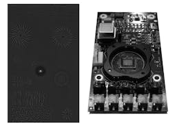
A simple implementation is another advantage of the diffraction approach. Initial tests were performed with a commercial array and a custom diffraction grating but it should be possible to fabricate the system on-chip using an additional step to the process (Fig. 2). Melding the system construction into the chip creation process has a number of advantages, from elimination of alignment issues that a lens requires to lowering system costs.
Figure 2. Rambus placed its special refraction grating (a) over a commercial photodiode array (b). The test grating had a number of different patterns, allowing the company to test different system configurations.
Moving the overall imaging system down to the chip level can lead to some interesting applications. For example, including multiple sensors on the same chip or integrating the sensor on the same chip as the supporting DSP opens up interesting possibilities. The test grating was designed for the visible spectrum, but diffraction gratings that span a narrower spectrum are easier to make. The overall cost of a sensor is a fraction of a refraction-based solution, so spreading a dozen sensors around a system could well be a practical and useful alternative.
Tiny Rambus Lensless Camera Could be Added to Any Electronic Device
Technology Editor Bill Wong interviews Patrick Gill, Senior Research Scientist, about RAMBUS' lensless camera system.
About the Author
William G. Wong
Senior Content Director - Electronic Design and Microwaves & RF
I am Editor of Electronic Design focusing on embedded, software, and systems. As Senior Content Director, I also manage Microwaves & RF and I work with a great team of editors to provide engineers, programmers, developers and technical managers with interesting and useful articles and videos on a regular basis. Check out our free newsletters to see the latest content.
You can send press releases for new products for possible coverage on the website. I am also interested in receiving contributed articles for publishing on our website. Use our template and send to me along with a signed release form.
Check out my blog, AltEmbedded on Electronic Design, as well as his latest articles on this site that are listed below.
You can visit my social media via these links:
- AltEmbedded on Electronic Design
- Bill Wong on Facebook
- @AltEmbedded on Twitter
- Bill Wong on LinkedIn
I earned a Bachelor of Electrical Engineering at the Georgia Institute of Technology and a Masters in Computer Science from Rutgers University. I still do a bit of programming using everything from C and C++ to Rust and Ada/SPARK. I do a bit of PHP programming for Drupal websites. I have posted a few Drupal modules.
I still get a hand on software and electronic hardware. Some of this can be found on our Kit Close-Up video series. You can also see me on many of our TechXchange Talk videos. I am interested in a range of projects from robotics to artificial intelligence.


