Members can download this article in PDF format.
What you’ll learn:
- How advanced SoC designs are replacing board-level systems.
- How an eFPGA can empower a system’s design.
- Considerations for eFPGA selection.
Developing advanced embedded systems is becoming more and more challenging to the designer. Functionality and connectivity create layers of added integration and complexity that often make it difficult to provide an optimum logic architecture to manage a given system, especially if it’s a system-on-chip (SoC). Let’s explore the anatomy of an embedded FPGA (eFPGA) and how to achieve the best optimization of silicon resources with the maximum amount of flexibility.
If we strip an FPGA into its component parts, we find primarily a core, typically containing the logic, memory, other macros such as DSP, an interconnect grid of wires, switches, and other compute elements, arranged in a grid or matrix. The I/O ring usually contains high-speed interfaces to the physical world, such as SerDes, LVDS, CMOS, and TTL interfaces. An eFPGA is, in essence, just the core of an FPGA without the I/O ring.
When it comes to the integration and functions required in an IC design, we find many IP blocks that must be integrated. Typically, a microprocessor (or 16!), phase-locked loops (PLLs), memory controllers, various buses, cache controllers, and the like would be in the mix. However, with the larger integration of logic functions and IP blocks, there needs to be a way of changing or updating an IC after production in a cost-effective manner.
Advanced SoC Designs Replacing Board-Level Systems
We’re entering an age where lots of legacy PCB-mounted ICs are getting mopped up and placed into a single monolithic IC or chiplets as an SoC. One issue is that IC design teams have the potential of missing a market area or a timeline if they don't incorporate the correct features, or they end up finding bugs in portions of the design.
An FPGA has been traditionally used to either prototype an IC, add flexible functionality to a design on a PCB, or just integrate all of the simpler I/O and control functions (and fix/add any last-minute requirements).
Since the advent of higher levels of integration, we’ve encountered massive bandwidth bottlenecks and I/O constraint issues, such as the inability to physically bond out enough I/Os in the space given on an IC package.
For instance, we’re seeing BGA packages of 2048+ I/Os at 0.5-mm pitch and below on a PCB, which causes a whole number of issues. These include physical pin density, routing congestion, layer counts with lots of micro-vias and stackup/lamination issues, and speed issues leading to signal-integrity problems such as simultaneous switching noise and crosstalk.
In addition, I/Os burn power and consume a lot of silicon real estate, while requiring separate power rails for all of the different I/O standards. Though every effort has been made to ensure accuracy of information contained herein, features, specifications, and technical information are subject to change without notice.
With all of this in mind, we need to think about how we can push past design limitations going forward. Offering a solution to these issues, an eFPGA is a matrix of LUTs/memory/DSP/compute elements that can be configured to be any size within the limits of the semiconductor die and real-estate requirements. It also provides a nearly limitless number of I/O interface pins—as many as the semiconductor design rules allow.
How an eFPGA Can Empower a System’s Design
It’s quite common to see a square design with 1,000 I/Os per side, giving a total of 4,000 user I/Os. An implicit advantage of using an eFPGA is that you can run at internal IC speeds, with no I/O bound interface limitations through LVDS, SerDes, CMOS, and others, along with very wide bus interfaces. This massively benefits designers, as they can run at system speeds on the IC die and have large buses to push data in or out of a definable logic/compute element. This definable logic can be designed after the IC has gone for tapeout and can be updated in the field or at production time, customizing the product as required.
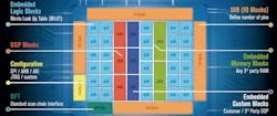
For example, Figure 1 shows that Menta's eFPGA is composed of smaller elements, with the I/Os and the components making up the Matrix. The I/O block contains optional registered I/Os with D flip-flops (D-FFs) so that the design can be clocked and timing can be closed at the interface level.
The embedded Custom Block (eCB) is a customer-specific definable function or hard macro that can be integrated into the matrix. This might be some definable AI or convolution function that’s proprietary, or a mixed-signal Digital/Analog block with a Digital interface (this being a feature of Menta's product offering).
The Configuration I/O is the interface in which the user programs the eFPGA bitstream with their customizable logic, and the DFT I/O is the Design for Test interface so that the eFPGA may be fully checked for design flaws after manufacturing, along with an embedded Logic Block (eLB). The DSP block is a DSP element containing a pre-processing FIR/IIR filter block and the usual Multiply/Accumulate functionality, which can be cascaded to make up larger DSP elements.
The embedded Memory Block (eMB) is an instantiated memory from the silicon foundry or a third party and can easily be integrated into the eFPGA definition. In addition, an Interconnect grid of wires and switches connect these elements together to make up the defined circuits and function. This isn’t shown in Figure 1 for brevity, but it can be assumed to be embedded where the grid lines are located. (Definable in an eFPGA means at design time/specification time and not after production.)
Addressing Programmable Logic
When it comes to programmable logic, the key is in the lookup tables (LUTs) that are part of the eLBs. A LUT is really a set of multiplexers that allows for the individual addressability of any input bit. It can create any combinational logic required by the user.
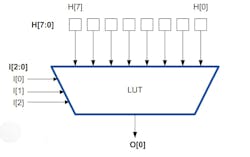
That task is accomplished by hardwiring the inputs of a LUT to a predetermined value and then using the inputs to the LUT to provide the correct logic output by addressing the appropriate individual bit. Figure 2 shows an example of a simple LUT that has three inputs I[2:0], eight hardwired inputs H[7:0], and one output O[0].
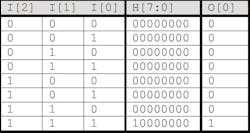
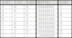
If we create a truth table (Fig. 3) of this, whereby we want to implement an AND gate (O[0] = I[2].I[1].I[0]), we can see that by addressing the element I[2:0] = 3'b111, we return bit H[7] of the LUT. Figure 4 looks at a more complicated function, O[0] = (/I[2]./I[1])+I[0].
As can be seen in Figures 2, 3, and 4, a LUT can be configured to map to any logic function as required. In essence, a lookup table is a one-data-bit ROM configured to create logic functions. The LUT can be mapped to any truth-table mapping function.
The inputs to the LUT are the logic function’s inputs and the contents from the lookup from the ROM give the logic equivalent outputs. In this example, we only have a 3-input LUT, but in more complex devices we have 4-, 5-, 6-, 7-, and even 8 input LUTs that make the LUT sizes increase with inherently longer delays.
There are various optimal sizes for LUTs, which are chosen by the manufacturers of the eFPGA and FPGAs to best fit the tradeoff between the logic-density requirements and speed. The “H” bits are known as “configuration bits” because they configure the function of the eFPGA's logic mapping. The LUT is the combinational logic part of the puzzle in the eLB.
However, there's another part of the puzzle—the D-FF—since most designs are synchronous (clocked) designs. All that’s required is to add a D-FF to the output of the LUT block (O[0]) so that the logic can be registered.
More Elements in the Matrix Mix
There are other elements within the eLB but that requires a lot more explanation and is not relevant to this level of description. The D-FFs have the ability to be SET and RESET, and the choice of which edge is used to clock can also be assigned. One more important element is the Switch Box, basically a cross-point switch that can connect any input to any output with configuration bits to program its function.
For example, a 16-I/O switch box would have four I/O on either side of a square and be able to route any of the points to another point. Switch boxes are custom-crafted to the architecture of the eFPGA/FPGA with various optimizations for speed/power/route-ability. The switch boxes are wired to metal lines and to the inputs and outputs of the eLBs (LUTs, etc.) to provide a routing path between the LUTs, memory, DSP, and compute elements.
Arranging all of these elements on a grid of wires, the LUTs, memory, DSP, and compute elements, along with the switch boxes, make up an eFPGA. There is also the storage of the “configuration bits,” which is where manufacturers differ in their strategies.
Most eFPGA and FPGA providers use SRAM bitcells, while Menta decided to employ D-FFs. There are some very good reasons for using D-FFs. Foremost, they’re typically more radiation-tolerant due to their nature as a master-slave system, so if a stray particle hits one of the elements, it’s unlikely to cause corruption. An SRAM cell has a dense array, susceptible to a stray particle that can flip the value of a bit.
As process geometries shrink, this is becoming more of an issue due to the thickness of the oxides and metal not being able to disperse the stray particles. Since Menta has standard D-FF at the heart of its technology, there’s no reason why a user can't use triple module redundant (TMR) techniques with the understanding that an area and speed penalty ensues when implementing a design this way.
Lastly, SRAMs require proprietary libraries from a Silicon Foundry which, most of the time, forces eFPGA providers to design their own bitcells. This creates another path for potential issues in the design.
The configuration SRAM needs some fairly complex logic to shift data bits through them as well as to address them. SRAM cells are also more prone to manufacturing errors since they push the boundaries of semiconductor manufacturing technologies as they use the highest packing density techniques (very small geometries). On a side note, yielding SRAM requires redundancy, which is cumbersome for eFPGAs. All in all, and thanks to architecture patents, Menta’s D-FF implementation doesn’t lead to a silicon area penalty compared to SRAM-based eFPGA IPs.
Another advantage of using D-FF is that Menta's eFPGA may be synthesized very quickly into a customer's product. All of the elements are standard cells. You can use whichever semiconductor foundry library that’s available and synthesize your custom eFPGA IP into your design quickly.
Other vendors provide “hard” macros whereby they must pre-qualify their IP blocks in a particular process/foundry geometry. That can take lots of time since they have to do layout, a netlist comparison, and timing and parasitic extraction before being able to commit a design to a particular process/foundry geometry.
Menta can provide the eFPGA verilog/VHDL netlist immediately to the design team so that they’re able to start integrating and doing floorplanning, as well as optimize their IP requirements (eLB/DSP/MEM/eCB mix). Obviously, there are guidelines on how the layout is done, and Menta provides this as part of the deliverables of what’s called “soft” IP. The company can also provide a service for layout of the IP if required.
DSP Blocks in eFPGAs
The DSP blocks in eFPGAs comprise a synchronous multiply-accumulate architecture that’s wholly based on logic. The iterative nature of these devices can be incredibly fast, and unlike a CPU/GPU, they don't need to have instruction streams to direct how the iterations are performed. In a CPU/GPU architecture there must be a Fetch-Execute-Store process where the CPU/GPU fetches an instruction, decodes the instruction, performs the operation in an ALU, and then stores the data back into memory or registers.
There’s a heavy cost to doing DSP operations in a CPU/GPU—basically, the memory loads and stores along with instruction decodes. A CPU doesn’t lend itself to a streaming DSP capability very well. The way in which hardware-based DSP architectures differ is that they’re doing bitwise mathematics in native standard-cell gates.
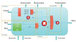
Figure 5 shows a DSP block and its constituent parts. On the left, we have the inputs A and B as bit vectors to do the math on, and Cin as a supplemental Carry input. We will ignore the green “FIR” box for now (assume the signals pass straight through it).
A and B will eventually be passed onto a multiplier as AF1and BF1, which will produce an intermediate product; let's call it P1. P1 is then taken into a Math block—it can be added to P3 where P3 was the last result (i.e., a value held in an accumulator). The output of P2 can have its sign changed, too, to provide the desired output.
In effect, the simple math function described is:
P = (A * B) + LAST_VAL, or
P = (A * B) - LAST_VAL
Let's not forget about the Carry input Cin. By adding a carry input to the addition, we can consider overflows from other previous calculations. Because the Carry is able to be shifted, we can change the carry's significance to the input as well. We call this Cin a “Pre-adder” since it can have different weightings/significance.
When looking at the Pre-adder block, you will notice that in the path before AF1, there’s an arithmetic block with unary sign “inversion” capabilities. This means that we can effectively change the input on Cin or A to become negative.
This now allows us to add the new math functions to the capability via the pre-adder. The equation becomes:
P = ((±A ± Cin) * B) ± LAST_VAL
Not to overcomplicate things, but the pre-adder has more capabilities than I've shown here. However, this would take us beyond the scope of this article. The FIR/IIR engine is a patented Menta technology that provides finite-impulse-response or infinite-impulse-response filtering, a common requirement for DSP algorithms.
Suffice to say that it’s a pre-process that could be used for harmonic or spur removal in the original signal and comes for free as part of the DSP block. It can be bypassed if not needed.
The Menta DSP Block also provides a “Cascade” ability that enables the DSP blocks to be daisy-chained together to provide a larger/wider “DSP” element. The obvious penalty is that the daisy-chained DSP function has been moved on to another pipeline stage. On the application side, there are a wide number of use cases for DSP mathematics. This would include:
- Convolution
- Filtering
- Modulation and demodulation
- Mixing/summing/decimation
- Image processing (kernel mathematics)
- Matrix mathematics (real and complex number math is capable in the DSP block!)
- FFT, DFT, correlation, etc.
- SDR (software-defined radio)—I/Q schemes
Tools and Workflow
Once you have an eFPGA IP that’s been designed, you now want to do some FPGA work for your application. This would include writing RTL (the application at hand), synthesizing the logic, place and routing the design, and extracting timing as well as static timing analysis.
Menta has a set of internally developed tools called Origami, a full development suite for implementing a design. This suite of programs is integrated under an umbrella GUI, but it can also be run individually at the command prompt using TCL/TK scripts.
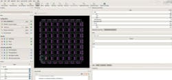
Many designers are used to automation in their workflow using TCL/TK scripts. Origami can be easily integrated into such a flow (Fig. 6). Origami is able to read all RTL languages (Verilog, System Verilog, and VHDL in all their defined standards), perform automatic hierarchy recognition, do synthesis into an internal netlist, perform optimized place and route (based on your I/O mapping), and generate a mapping file for the configuration bitstream data.
In addition, Origami does static timing analysis and will provide a back-annotated SDF netlist for post place-and-route simulation. The timings are extracted from sign-off EDA tools for the eFPGA IP design, thanks to the third-party standard cell libraries, and they remain under the full control of the customer.
Origami can optimize logic to use DSP elements where it sees fit, too. The user chooses what kind of optimization they want to map to DSP blocks to implement designs highly optimized for speed where math is concerned.
Once Origami completes the workflow, a bitstream file is produced. This bitstream would then be written to the eFPGA’s programming interfaces to configure the eFPGA for its end function as per the user's design/application. This enables the host to store multiple bitstreams with different functions. These may be chosen and written (downloaded) to the eFPGA as required, providing a choice of hardware functions.
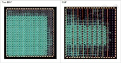
By carefully selecting your mix of DSP and LUTs, you can achieve better packing ratios and functional speeds (Fig. 7). This optimization process is iterative and depends greatly on designs; at this point, you need to engage with the eFPGA vendor.
In Menta's case, by the nature of its product design, this iteration process can be a matter of days or even hours if the company works on-site with the customer. As you can see in the routed floor plans in Figure 7, the utilization is much smaller on the DSP architecture. That’s why it’s so important to engage with your eFPGA vendor at the planning phase and have them involved in your design cycle.
Considerations When Selecting an eFPGA
When choosing an eFPGA, you should be aware of your range of applications and what you want to achieve. eFPGA vendors provide a vehicle with which you can add flexibility to your custom IC, but you have to be aware of the limitations of what’s achievable in an eFPGA. Clock speeds will be less than raw standard cell ASIC design, and porting a portion of your current ASIC IP (Verilog and VHDL) will likely require some custom work.
Typically, we find that ASIC IPs use gated clocks, which is a big “NO” for FPGAs, so expect some handcrafting. Optimization of code can significantly reduce logic usage as well, because an eFPGA/FPGA has larger blocks to which the logic is mapped. FPGAs map into LUTs and D-FFs, whereas a custom ASIC maps into standard or full custom cells.
For DSP applications, you would need to carefully craft your DSP code and/or define an optimal architecture to take advantage of the DSP elements if you wish to get the highest performance/utilization of elements. You must also be aware of the programming interface and be able to send in a bitstream from your design (ROM, CPU, etc.), with a solid design-for-test plan and strategy.
The benefits of an eFPGA are flexibility, design reuse, the ability to make post tapeout changes to fix bugs or change algorithms, and the possibility for a customer to make a more general ASIC that can be customized for different products.

