NOR flash storage provides a performance edge and reliability compared to NAND flash but current interfaces tend to limit performance. Applications such as high resolution photography and automotive telematics are pushing past current limits.
Related Articles
- How HyperBus Delivers 330 Mbyte/s Using A Dozen Signals
- Serial NOR Flash Doubles Embedded-App Programming Speed
- Dual-Quad SPI Flash Family Meets Automotive Instrument-Cluster, HMI Needs
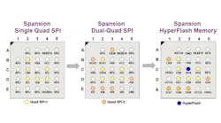
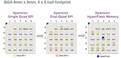
Spansion’s new HyperFlash NOR flash memory chip is designed to meet the requirements for these high performance applications. This means faster camera capture cycle times and fast boot times for automotive technology. It can be access using quad SPI (QSI), dual QSI and Hyperbus (see How HyperBus Delivers 330 Mbyte/s Using A Dozen Signals). This can be handled by a single 6 mm by 8 mm chip (Fig. 1). The 24-ball, 5 by 5 footprint provides an upgrade path depending upon which interface needs to be employed.
HyperFlash is available in 1.8 V and 3 V versions. The 1.8 V HyperBus clock rate is 166 MHz. The transfers are double data rate (DDR) that delivers a 333 Mbyte/s transfer rate. It supports a wrapped burst mode of 16, 32 and 64 bytes. The HyperBus uses a 6 byte command/address header for each transaction following by read or write data (Fig. 2).
The 1.8 V version has a differential clock (CK/CK#) while the 3 V version uses a single clock line. It also has a lower maximum transfer rate of 100 MHz or 200 Mbytes/s. The typical QSPI interface delivers data at 40 to 66 Mbytes/s. Parallel NOR flash runs at rates from 70 to 96 Mbytes/s.
Spansion is initially delivering HyperFlash in 128, 256 and 512 Mbit versions. Even the largest can be read completely in a fraction of a second. They are fast enough for eXecution In Place (XIP). The chips are available with automotive temperature ratings.
HyperBus fills a large performance gap with an interface that should be easy to implement on most hosts unlike more powerful interfaces like MIPI/M-PHY and PCI Express. These serial interfaces operate at a significantly higher clock rate and using more sophisticated protocols. They have their advantages but tend to be overkill for many midrange embedded applications.
HyperBus fits above I2C and SPI. These use fewer lines but at a much slower transfer rate. There are still plenty of applications for these slower interfaces and many devices that support them. Devices that support HyperBus will probably include support for these as well.


