Power Efficient Multicore SoCs Handle Vision and HMI Chores
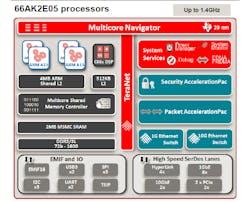
Texas Instruments’ (TI) 28-nm AM5K2Exx and 66AK2Exx multicore SoCs (Fig. 1) address a range of applications from computer vision to user interface. They can handle chores from cloud computing to embedded industrial applications. The Keystone II platforms are based on Arm Cortex-A15 cores that are tied together using TI’s TeraNet fabric. The cores have a 4 Mbyte shared L2 cache. The L2 has ECC support as does the DDR3/3L controller. The DSP has a 512 Kbyte L2 cache.
Unused cores and peripherals can be powered down. The low power platforms use under 10 W for the 66AK2Exx and 8.5 W for the AM5K2Exx. They typically use under 8 W at 55°C. The chips are designed to handle 100K power-on hours (POH). They also support junction temperatures up to 105°C.
The system has major connectivity on chip. There is a 5-port, 1 Gbit and a 3-port, 10 Gbit Ethernet switch along with eight 1 Gbit and two 10 Gbit Ethernet interfaces. The system also has four TI HyperLinks that can link multiple TI chips together. There is also a pair of 4-lane PCI Express Gen 2 ports.
The platform includes security and network accelerators. The Security AccelerationPac provides hardware-based encryption and random number generator. The Packet AccelerationPac handles L2 through L4 routing.
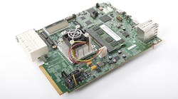
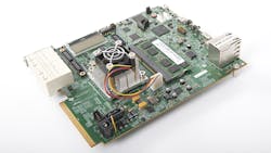
Developers can take advantage of the development platforms like the AM5K2Ex EVM (Fig. 2).
Texas Instruments provides software development kits (SDK) as well as application libraries. It support mainline Linux distributions as well as LTS (long term support) implementations. Commercial RTOS solutions are available from a number of third parties such as Green Hills Software and Wind River. The two chip families are supported by TI’s Code Composer Studio as well as third party tool suites.


