GPU Targets Deep Learning Applications
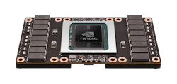
The 16-nm FinFET-based Tesla P100 (Fig. 1) is the next-generation GPU from NVidia. It targets a range of applications including deep learning, delivering 12 times the performance of the previous GPU generation, NVidia’s Maxwell architecture. The Tesla P100 incorporates many new features and technologies, including High Bandwidth Memory 2 (HBM2) and Chip-on-Wafer-on-Substrate (CoWoS) technology.
The Tesla P100 consists of 15.3 billion transistors. HBM2 is the next generation of stacked, on-chip memory. AMD used HBM in its latest Radeon R9 series. NVidia also added unified memory support for CPUs and GPUs that is similar to AMD’s Heterogeneous System Architecture (HSA). This allows the CPU and GPU to use the same pointer structure simplifying CPU and GPU programs. The improved memory system deliver a 3x memory bandwidth performance boost. The Tesla P100 ECC memory runs at 720 Gbytes/sec.
Deep learning technologies employ neural networks with dozens to thousands of levels. The new half-precision instructions of the Tesla P100 allow it to deliver more than 21 TFLOPS of peak performance. It also delivers 5 TFLOPS of double-precision and 10 TFLOPS of single-precision performance.
The Tesla P100 is designed to work in multi-chip configurations linked together using the new NVLink interface, which runs at 160 GBytes/s—or five times faster than PCI Express Gen 3. Each chip has four NVLinks, allowing a rectangular layout without additional circuitry.
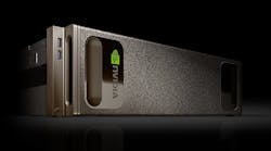
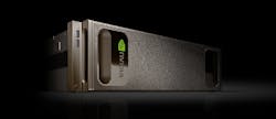
NVidia packs eight Tesla P100 GPUs into the new DGX-1 system (Fig. 2). The compact, rack mount system also includes 7 Tbytes of SSD storage and a pair of Intel Xeon CPUs. Each GPU has 16 Gbytes of memory; all comprise a hybrid cube mesh. DGX-1 has a pair of 10-Gigabit Ethernet ports and a quad 100Gbit/s InfiniBand port. The 3U system uses only 3,200 W and is priced at $129,000.
The Tesla P100 GPU shows significant performance improvement compared to CPUs for some applications. One such example is the AMBER molecular dynamics code, where a single Tesla P100 has comparable performance results as 48 dual-socket CPU server nodes. Trainingfor the AlexNet deep neural network can be handled by eight interconnected Tesla P100s or 250 dual-socket CPU server nodes.
The Tesla P100 and DGX-1 are supported by the new NVidia SDK that includes NVidia’s CUDA 8. It can take advantage of HBM2 and NVLinks on the Tesla P100. The SDK also includes the new graph analytics library, nvGRAPH. This can be used for applications such as robotic path planning, cyber security, and logistics analysis.
The cuDNN library version 5 is a GPU-accelerated Deep Neural Network (DNN) library. It includes support for recurrent neural networks that are used for data that includes sequential streams (such as audio and video). The cuDNN library is used by leading deep learning frameworks including Google's TensorFlow, UC Berkeley’s Caffe, the University of Montreal’s Theano and NYU’s Torch.
The Tesla P100 GPUs can be used in many application areas, including automotive. A pair of Tesla P100 GPUs can be found on the Drive PX 2 announced at the 2016 Consumer Electronics Show. The Drive PX 2 deliver 8 TLOPS of performance.
The Drive PX 2 is the heart of the self-driving car (Fig. 3) for the RoboRace Championship. Teams get identical hardware that can then be customized with their own software, typically built using tools like the NVidia SDK. The cars include large array of sensors including radar, lidar, cameras, GPS, and high-definition mapping support.
NVidia’s Tesla P100 represents a major improvement over previous NVidia GPUs. It is optimized for a many applications, especially deep learning. It will prove useful in the cloud and corporate arenas with the ability to restart GPU computation, allowing a system to support multiple users.
Looking for parts? Go to SourceESB.


