Tweet This: FPGA Taps 2.5D Tech For 10,000 Connections
Fig 1. The Xilinx Virtex-7 2000T, at 6.8 billion transistors, is the largest FPGA around (a). It’s implemented using 2.5D Stacked Silicon Interconnect technology (b).
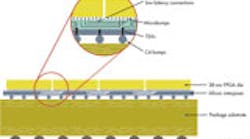
Fig 2. Xilinx’s Stacked Silicon Interconnect technology employs a silicon interposer layer between multiple chip slices and the package substrate. The layer links slices together and passes chip connections to the outside world.
Twitter is the Internet’s haiku. Traditional Japanese haiku consists of 17 “on” or syllables delivered in three phrases of five, seven, and five on. It is poetry that can be beautiful, concise, and insightful.
Twitter microblogging tweets are less formal and limited to 140 characters. This limitation stems from Short Message Service (SMS) text messages, which originated with cell phones. Tweets tend to take advantage of abbreviations, Internet slang, short URLs, and Twitter user names and hash (#) tags.
This leads to interesting tweets like: “FPGA from @Xilinxinc uses 2.5D technology - 10,000 Connections Between FPGA Slices: http://bit.ly/txBCPf.” This tweet happens to be about an online article I wrote about Xilinx’s new Virtex-7 2000T FPGA (Fig. 1).
2.5D FPGA
The Virtex-7 2000T packs in 6.8 billion transistors using four chip slices and links them together using a silicon interposer layer (Fig. 2). Unlike conventional multichip packages, the connections between these FPGA slices do not require I/O buffers. Along with 65-nm interconnects, the technology enables more than 10,000 connections between slices. It also meshes well with the layout of an FPGA that has a regular rectangular interconnect fabric.
The silicon interposer layer is essentially a multilayer chip, but it does not include any logic or interface elements. Through-silicon vias (TSVs) allow the top layer of chips to be connected to micro bumps at the bottom of the interposer. The micro bumps are linked to the ball-grid array (BGA) balls at the bottom of the package. These connections normally have I/O drivers unless they provide power connections.
The FPGA chip slices use Xilinx’s 28-nm technology with 13-Gbit/s serializers-deserializers (SERDES). The interposer uses 65-nm technology, but it still provides plenty of connections between chips. The 2.5D designation is implied by the 2D array of slices and the limited stacking employed with the interposer.
Multiple slices and layers add to system complexity, but there are advantages to the approach. Lower power is one advantage. So is the ability to create large chips. Now, FPGAs can move into the areas dominated by application-specific standard parts (ASSPs) and ASICs.
The 10,000 connections between slices change the game. Current chips use the same slices, but it isn’t required. Xilinx can substitute lower-power FPGA slices, but a slice could contain almost any logic or silicon technology. In fact, there will be a variant that has 28-Gbit/s SERDES on its own slice. This configuration has three FPGA slices and puts two of the SERDES slices at either end of the array.
Designers will employ Xilinx’s usual ISE Design Suite development tools, which account for the unique layout and timing characteristics of the Virtex-7 2000T. Designers also can partition designs to take advantage of different performance slices.
Track my tweets on Twitter at @altembedded, which also is the name of my blog. Check out the rest of the Electronic Design crew and, of course, @electronicdesgn (sic, due to Twitter name length limitations).
Twitter
www.twitter.com
Xilinx
www.xilinx.com

