Coin-Sized 3D Printer’s Tiny Photonic Chip Turns into Laser-Steering “Engine”
What you’ll learn:
- How this 3D printer differs in technical approach and size from “conventional” units.
- How the laser beam is managed and steered to cure the unique resin.
- The results that were achieved using this proof-of-concept 3D printer.
It’s well known that additive manufacturing (AM) of various distinct types and using a range of materials, often collectively referred to as “3D printing” in popular terminology, has dramatically changed if not revolutionized (a word I don’t use casually) prototyping, model building, repair and maintenance, and even some production-scale manufacturing lines.
AM has also enabled fabrication of objects that would be difficult or impossible to create using traditional forming, molding, casting, etching, or machining operations. While the size of these 3D printers varies, they’re typically tabletop size measuring a few feet on each side.
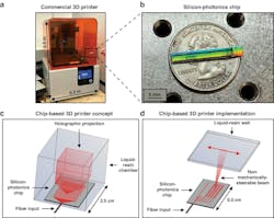
But that printer-size requirement may be scaled down, especially for small objects. Researchers from MIT and the University of Texas at Austin worked together to develop and demonstrate a tiny proof-of-concept, chip-based 3D printer by combining silicon photonics and advanced photochemistry to create what they maintain is the first such printer.
The system developed by MIT consists of only a single millimeter-scale photonic chip without any moving parts. It emits reconfigurable visible-light holograms up into a simple stationary resin well that cures into a solid shape when light strikes it, thus enabling non-mechanical 3D printing. You can think of it as a “personal” 3D printer.
Breakthrough in Additive Manufacturing: 3D Printer Principle and Design
The prototype chip has no moving parts, and instead uses an array of tiny optical antennas to steer a beam of light. The beams of these antennas aren’t steered by MEMS-type micromirrors. Rather, the research team developed an integrated optical-phased-array system to steer the beams of light by using a series of microscale optical antennas fabricated on a chip using semiconductor manufacturing processes (Fig. 1).
The silicon-photonics chip sits at the bottom of a chamber of resin and projects a reconfigurable, programmable visible-light hologram upwards into the resin, causing the resin to selectively polymerize into a solid print in the shape of the desired object. The phase and amplitude distributions necessary for generating a desired holographic image are closely approximated by discretizing these ideal continuous distributions into local one-dimensional phase gradients.
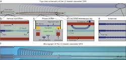
The silicon-photonics chip is based on a visible-light integrated optical phased array consisting of a liquid-crystal-based, cascaded-phase-shifter architecture that linearly controls the relative phase applied to an array of antennas. By speeding up or delaying the optical signal on either side of the antenna array, they were able to move the beam of emitted light in a desired direction The beam projects up into a liquid resin that has been designed to rapidly cure when exposed to the beam’s wavelength of visible light.
A single waveguide on the chip conveys the light from the off-chip laser. Running along the waveguide are tiny taps that tap off a little bit of light to each of the antennas. These tap couplers, placed with a pitch of 20 μm and with increasing coupling lengths, uniformly distribute the light from the bus waveguide to 16 vertically stacked and horizontally offset tap waveguides. The tap waveguides then route to 16 grating-based, uniform-perturbation, 400-μm-long antennas with a 2-μm pitch to emit the light out of the surface of the chip (Fig. 2).
The researchers used liquid crystal to create the compact modulators they integrated onto the chip. The material’s unique optical properties enable the modulators to be extremely efficient and only about 20 microns in length.
In a nematic liquid-crystal medium, the refractive index varies based on the orientation of the liquid-crystal molecules with respect to the propagation direction of the light. Thus, by applying an electric field across the liquid-crystal region to orient the molecules in the direction of the applied field, the index of the liquid crystal media can be actively tuned. This, in turn, changes the effective refractive index of the optical mode in the waveguide and causes a linear phase shift to the antennas. In this way, they can precisely control the amplitude and phase of light being routed to the antennas.
Evaluation and Testing of the Chip-Based 3D Printer
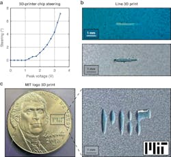
Using this non-mechanical beamsteering capability, they first demonstrated 3D printing of a line into the resin by sweeping the voltage applied to the liquid-crystal-based phase shifter. As the voltage applied to the phase shifter is increased, the refractive index of the liquid crystal relative to the mode in the phase shifter ramps up, leading to lower confinement of the mode in the bus waveguide. To compensate for some nonlinearities, they printed for longer times at higher voltages than for lower voltages, to ensure uniform curing along the line (Fig. 3).
The exposition of the 3D-printer core developed by the MIT team had to be examined alongside the important role of their partners at the University of Texas. That chemical-centric team developed the required specialized resin, which can be rapidly cured using wavelengths of visible light, also claimed to be a first. The complete 3D system uses visible-light lasers with resins that’s able to cure in the same wavelength band. This was a crucial development that pushed the chip-based 3D printer into reality.
To demonstrate the system’s ability to print arbitrary 3D patterns in two dimensions, they began with single-line prints as a building block. Then, to transition from these single-line prints to arbitrary two-dimensional patterns, they used the resin well’s mechanical positioning stage to move the well with micron-scale precision in the second dimension after printing each one-dimensional line in a desired pattern. They even printed the MIT logo by creating each line in the print from a subset of the single-line voltage range.
The project is described with crispness and clarity in their 11-page paper “Silicon-photonics-enabled chip-based 3D printer” published in Nature’s Light: Science and Applications. It highlights the five objectives of the project and what was achieved, as well as the technical details and specifics.
This work was funded, in part, by the U.S. National Science Foundation, the U.S. Defense Advanced Research Projects Agency, the Robert A. Welch Foundation, the MIT Rolf G. Locher Endowed Fellowship, and the MIT Frederick and Barbara Cronin Fellowship.
Read more articles in the TechXchange: Silicon Photonics.
About the Author

Bill Schweber
Contributing Editor
Bill Schweber is an electronics engineer who has written three textbooks on electronic communications systems, as well as hundreds of technical articles, opinion columns, and product features. In past roles, he worked as a technical website manager for multiple topic-specific sites for EE Times, as well as both the Executive Editor and Analog Editor at EDN.
At Analog Devices Inc., Bill was in marketing communications (public relations). As a result, he has been on both sides of the technical PR function, presenting company products, stories, and messages to the media and also as the recipient of these.
Prior to the MarCom role at Analog, Bill was associate editor of their respected technical journal and worked in their product marketing and applications engineering groups. Before those roles, he was at Instron Corp., doing hands-on analog- and power-circuit design and systems integration for materials-testing machine controls.
Bill has an MSEE (Univ. of Mass) and BSEE (Columbia Univ.), is a Registered Professional Engineer, and holds an Advanced Class amateur radio license. He has also planned, written, and presented online courses on a variety of engineering topics, including MOSFET basics, ADC selection, and driving LEDs.
Voice Your Opinion!
To join the conversation, and become an exclusive member of Electronic Design, create an account today!

Leaders relevant to this article:


