With the introduction of systems-on-a-chip (SoCs), the semiconductor industry has struggled with providing information on how to implement these devices while not overwhelming engineers with data. It is common today to find devices with documentation that exceeds 75 to 100 pages, which can be more accurately defined as a user manual than a datasheet. Simply trying to read the documentation and gather enough insight to use the device can take weeks, if not longer. Suppliers often provide an overview along with pin definitions to accelerate the process, but the task can be daunting for many.
In the beginning, suppliers often had schematics and a suggested layout for various functional applications. A functional application can be a block such as an arithmetic logic unit, frequency-to-voltage converter, or an FM demodulator based on a set of ICs. Most, if not all of these, come from the same vendor.
This file type includes high resolution graphics and schematics when applicable.
Classic examples of such collections (prior to the World Wide Web) were the highly acclaimed application handbooks. These were often in high demand and a prized possession of many engineers of the day. Often, they were kept in locked cabinets to prevent pilfering by other engineers. The books were written by the IC designers and application engineers responsible for these devices, which provided great insight into how to solve complex problems using such building blocks.
However, as higher levels of integration began to drive complexity, documentation became more focused since many devices now target specific applications, such as communications, computing, or signal processing. A processor datasheet might show the recommended power sequencing, memory timing, and I/O interfaces, but lack an entire motherboard schematic. It would provide all of the basic information required by the engineer, but not necessarily the subtleties of a real-world implementation.
This concept of providing application-specific implementation examples has been very prevalent in the software community through example code. It’s much easier to implement and deploy than hardware, but the concept is exactly the same. Code libraries can be extremely complex, and without a good understanding on how the authors intended the implementation, it can take a great deal of time to figure out when just using the documentation.
Evaluation Boards and Reference Designs
Suppliers quickly realized being competitive required more than simply supplying the datasheet. Many analog suppliers knew that evaluating a power-supply device or an amplifier would require an engineer to breadboard or prototype something in order to test the design. If a first attempt failed, the designer might move on to another vendor. However, by providing an evaluation board, or even simply a blank PCB and schematic, it would greatly increase the odds of a successful evaluation.
Now imagine devices such as FPGAs, multicore processors, or giga-sample data converters with hundreds of pins that need a great deal of support circuitry to function. Under these circumstances, there’s no option other than to supply some form of evaluation board. Most often, these were for sale by the vendor or a third party.
Evaluation boards were designed to provide access to most every feature of a component and, thus, have additional circuitry that may not be found in a final design. These tools are excellent for understanding what is possible with a device, and to try various options while making engineering tradeoff decisions.
However, following a successful evaluation, engineers often want a reference-design board and documentation illustrating the tradeoffs made to reach maximum performance. These differ from the evaluation designs, which were burdened with circuitry used for testing.
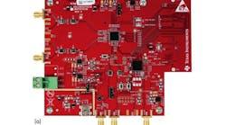
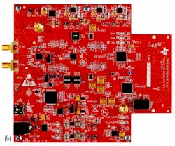
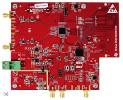
A reference design is as close as a vendor can get to a production application of a device while remaining general in nature. For example, an analog-to-digital converter (ADC) such as the ADC16DX370 has two different boards available: one that’s an evaluation module designed to exercise many of the features of this device, and the other a reference design board that implements a 700- to 2700-MHz dual-channel, super-heterodyne receiver subsystem (Fig. 1).
The reference design includes block diagrams, schematics, design files, test results, and more targeting of specific applications like software-defined radios (SDRs), communications, and test-and-measurement systems. The reference design shows a practical example of how the ADC should be used, and recommends additional components that will provide the best performance for the application—something that will save engineers a great deal of time. Even if an engineer chooses not to acquire a reference-design board, most times all of the supporting documentation is available for free on a vendor’s website.
Application-Specific Reference Designs (ASRDs)
With many new highly complex components being targeted to very specific applications, a new breed of reference design is emerging. Sometimes these are complete turnkey designs. They include everything required to produce the product, such as a bill of materials (BOM), Gerber or other format layout files, schematics, and documentation.
In some cases, application engineers have been tasked with solving a very specific problem for customers. In this situation, it’s sometimes best accomplished by assembling multiple development kits, evaluation modules, or reference-design boards into a system, and providing supporting tools and software to complete the design. This is another form of an ASRD, but utilizing a multi-board configuration.
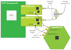
An excellent example of an ASRD is a phased-array RADAR receiver reference design, TIDA-00432, which utilizes an FPGA standard development kit along with multiple ADC and clock evaluation boards (Fig. 2). This also represents a good example because of the problem being addressed. In phased-array RADAR or other multi-antenna systems, it’s often challenging to accomplish correct converter alignment, also known as phase coherency.
With the introduction of the JESD204B data-converter interface standard, an engineer familiar with legacy parallel interfaces will be faced with developing an understanding of the new serial architecture and how it implements phase coherency between multiple converters. This can be quite a steep learning curve. Providing a working example of how to accomplish this feat can greatly decrease the time required to move from concept to a working system.
The design also provides test results taken from the actual hardware so that engineers can understand the system’s performance. Furthermore, the hardware is available from its respective vendors, allowing engineers to re-create the system described in the ASRD documentation.
Conclusion
As semiconductor devices continue to increase in complexity, more reference material will be required to ensure that engineers can develop a system in a timely manner. The examples provided are just the beginning of the various reference designs that may soon be available to engineers and designers. The intent of these products is to promote available solutions as well as accelerate the development of extremely complex products. As engineers continue to face ever-increasing requirements for their systems, ASRDs will help shorten the learning curve needed to use the latest solutions from semiconductor suppliers.
This file type includes high resolution graphics and schematics when applicable.
References
1. “Synchronization of JESD204B giga-sample ADCs using Xilinx Platform for phased array radar systems” (TIDA-00432).
2. ADC16DX370EVM, TSW16DX370EVM and reference design.


