Digital Modeling Yields Efficient Rigid-Flex PCB Design Processes
This file type includes high resolution graphics and schematics when applicable.
More than ever before, product experiences are being driven by customer interaction (i.e., seeing, touching) with the physical, mechanical model. The necessity to constantly satisfy the senses of the physical experience requires that printed-circuit-board (PCB) assemblies be smaller and denser to fit pre-conceptualized mechanical structures.
The mechanical model becoming such an influential factor has turned flexible electronics into an increasingly common, and significant, design objective. To gain this flexibility, designers often opt for rigid-flex PCBs, which combine both the rigid and flexible substrates of a PCB into a single design element.
Despite its numerous benefits, rigid-flex PCB design presents significant challenges in terms of effective, efficient execution. Among the many variables that go into the rigid-flex PCB design process, the greatest challenge faced by designers is ensuring that all flexible sections on the PCB fold in the correct way, while maintaining flex-circuit stability and product lifespan at the highest feasible degree of quality.
So how do you go about ensuring that your rigid-flex PCB folds as desired while fitting precisely into an existing mechanical enclosure? Let’s explore some of the current practices.
Child’s Play—The Paper Doll Approach
The most common method deployed by design teams to ensure that a rigid-flex PCB design will fit in an enclosure is the “paper doll” model of the PCB. These models, created from paper, are cut into what’s hoped to be an exact shape of the PCB in concept. This method has its roots in traditional PCB applications, but recently gained widespread use with the need to model flexible circuitry. Most PCB fabricators still promote this approach.
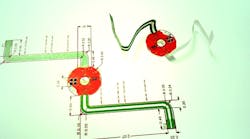
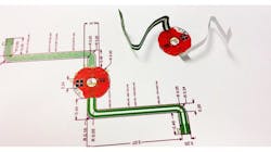
Figure 1 shows an example of a cardboard paper doll being used to model the mechanical fit of a stepper-motor controller. To create this model, the designer first made a 1:1 printout of the 2D PCB outline, then cut it into its final shape. To more accurately model the assembly and provide a more precise feel to the model, the designer glued a piece of cardboard to the paper model to approximate the thickness of the rigid parts of the PCB.
While effective at modeling an approximate shape of a rigid-flex PCB, the paper doll approach has a number of inefficiencies and problems in application, including:
• Imprecise thickness: The paper doll isn’t the same thickness as the rigid and flexible sections of the PCB. Therefore, it becomes very difficult to simulate the bending of the paper model because it will bend in its final application. This makes it incredibly challenging to get a clear idea about the fatigue or natural folding properties of the design.
• No 3D models: The paper doll doesn’t include all of the 3D component models that will appear in the final design. One must wonder how the presence of these models will change how the model folds, and whether a 3D model might interfere with the clearance required for the rigid-flex sections to fold properly.
• Costly 3D printing: To determine a correct board fit with an enclosure, it might be necessary to print the enclosure with a 3D printer. Depending on the complexity of a design, this can become a costly option to implement—it adds a layer of unnecessary expenses to a project that could have been simulated entirely in software.
Despite its widespread use, the application of paper doll models to simulate the real-world application of a rigid-flex PCB design is both imprecise and impractical. Designers who rely on this method to ensure a correct PCB fit with the mechanical enclosure risk the potential of design revisions and expensive prototype adjustments during the fabrication process. So, are more sensible and efficient approaches available to designers?
Digital-Modeling Efficiencies
Rather than build an inaccurate paper doll model, a more sensible approach is to handle all of the modeling and simulations directly in the digital software environment. Not only will this approach save time and money, it will also yield a more exact design that doesn’t depend on the imprecision of paper models.
In practice, there are currently two accepted methods to execute this approach: using a combination of mechanical computer-aided design (MCAD) tools and electronic computer-aided design (ECAD) tools, or using an ECAD tool alone with built-in 3D functionality.
MCAD/ECAD Modeling
This is commonly referred as the “sheet-metal method” because of its inherent similarity to designing a sheet-metal part. While relatively straightforward, one must be cognizant of the number of steps involved in this process.
The initial MCAD model of the product is designed alongside a sheet-metal component, which forms part of the assembly. Once the MCAD model is created, one or more fixed tabs model the rigid sections of the design, and stiffener is used for the flexible portions.
This method offers a precise, organized way to discover what area is available for the PCB substrate. However, this shape still must get into the PCB designer’s workspace. To complete the final steps in this process, you could use the “unbend” and “unfold” features in your MCAD environment to generate the necessary models. These could then be imported to your chosen PCB editor.
The generated data, which can be exported to a PCB editor as an IDF or DXF file, will provide the outline of the rigid-flex section of the PCB for further refinement in the ECAD environment. Once in the PCB editor, components are placed and an IDF file is generated again. Then the file is imported back to the MCAD environment, where the mechanical designer can refold the board substrate.
The process of positioning the board and components as a folder circuit is time-consuming, though, rendering this approach somewhat unidirectional from MCAD to ECAD. As a result, it may still be iterative and require close cooperation between MCAD and ECAD designers.
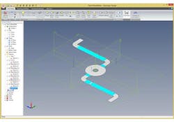
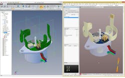
Figure 2 shows this in practice, with the rigid-flex PCB of our stepper-motor controller being modeled in the MCAD environments. The neon-blue highlighted sections are the “unbended” sheet-metal sections (representing the flattened flex-circuits). This unbended model is exported as DXF to the PCB design tool.
While the MCAD/ECAD translation process provides a more exact replication of a rigid-flex PCB, it does require the tedious process of translating design data back and forth between each design environment. What if you only had to use one design environment to accurately model and simulate your rigid-flex design?
ECAD Modeling with 3D
A more efficient way to design a rigid-flex PCB is to use an ECAD tool with 3D functionality. With 3D functionality built into the ECAD environment, designing a rigid-flex PCB requires fewer steps from design to completion, greatly reducing the amount of time invested in a design.
When using an ECAD tool with 3D functionality, the PCB layout and mechanical assembly are modeled together with the use of 3D STEP models. This allows designers to easily visualize the entire assembly, including the necessary mechanical enclosure and component models.
This process isn’t intended to replace a dedicated MCAD system. Rather, it’s a major step forward in improving workflows and lessening the time wasted modeling and simulating a completed product design. The ability to model both the PCB and associated mechanical enclosures and components provides designers with a high degree of precision when checking mechanical clearances in real-time 3D, ensuring that a board fits right the first time.
In addition to the above mechanical modeling capabilities, the use of ECAD software with 3D functionality provides access to the PCB’s dielectric and copper information. When utilizing this information in an MCAD environment, the mechanical designer has access to more detailed simulation options, including thermal and electromagnetic analysis.
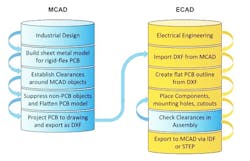
Figure 3 illustrates a typical workflow using ECAD software with 3D functionality. Once the PCB outline is generated, the electrical designer can define the needed layer stacks for the rigid and flexible sections of the PCB, and then assign these layers to appropriate areas on the design.
After completing this step, the bending and folding areas of the final product are defined, and can be examined and simulated in detail to ensure correct form. At this stage of the design process, it’s easy to verify if the flexible portions of a design are too short or long and adjust them accordingly.
Once the modeling process is complete for both the rigid and flexible parts of the PCB design, engineers can then place the needed components on the board, including connectors, heat sinks, LEDs, light pipes, and other mechanical models. During this process, it’s beneficial to have a STEP model of the final enclosure in the ECAD environment.
With this data at hand, the designer can actively check for clearances between the board, components, and enclosures all in real-time 3D, or perform a comprehensive design-rule check to identify design errors. With this integrated method, designers can expect to see a 50% reduction in the amount of time it takes to verify and validate the shape and folds of a rigid-flex PCB (Fig. 4).
Upon completion of the modeling and simulations in the ECAD environment, designers can transfer this data back to the MCAD software as a STEP model and begin the final process of combining the PCB with the completed mechanical design.
Compounding Design Efficiencies
In addition to delivering better boards, the 3D STEP models generated from the rigid-flex design (including folded, unfolded, and partially folded states) deliver more accurate and detailed documentation. Manufacturing engineers can use this enhanced documentation to develop clear assembly instructions for both the PCB assembly and the final product.
If desired, manufacturing engineers can even produce a video from the images generated in the ECAD environment. These videos can be used to train assembly personnel in the exact process required to fold the flexible circuitry. Implementing this process helps significantly reduce assembly time and errors, thus streamlining the entire design-to-fabrication process.
This file type includes high resolution graphics and schematics when applicable.
Despite the benefits, it’s important to note that like any other process driven by incremental improvements in technology, not even the most precise STEP models provide a 100% accurate picture of design intent. More advanced models and systems for streamlining the rigid-flex design-collaboration process between electrical and mechanical design teams are certain to appear down the road.
Design Success Through Digital Modeling
It’s clear that maximizing the efficiencies of your rigid-flex design process goes far beyond the currently accepted methods of prototyping PCBs and enclosures with paper-based models. Ensuring that your board fits the mechanical enclosure right the first time, while also maximizing the quality of your flexible circuitry, requires a more advanced workflow incorporating the use of 3D functionality in an ECAD environment. When it comes to remaining competitive and productive, don’t leave your designs up to chance. Use a digital modeling and simulation system for the most efficient rigid-flex design process.
To learn more about rigid-flex design, click here.
