7 Engineering Essentials for Printed Circuit Board Design Success
This file type includes high resolution graphics and schematics when applicable.
In this article, we’ll discuss seven basic (but critical) tips and strategies for beginners and masters alike. Pay attention to these tips during your design process, and you'll reduce spins, design times, and overall diagnostic hair-pulling for you and your team. So let's get started.
1. Bone Up on Fabrication Methods and Fab Chemistry
In this era of fabless IC companies, it isn’t all that surprising how many engineers don’t actually know the steps and chemistry involved in creating PCBs from their design files. This lack of practical knowledge can often lead a newer designer to make design choices that are more complicated than necessary. For example, a common novice mistake is to lay the board out in extremely precise geometries, using orthogonal trace bends on tight grids, only to find out that not every board shop has the capabilities to produce the design with sufficient reliability to sustain a lifetime in the field.
The shops that do have these capabilities may not provide the most economical pricing for the PCB. Did the design really need to be that complex? Could the board have been laid out on a larger grid, reducing the cost of the boards and improving the reliability? Other pitfalls for novice designers are unnecessarily small via sizes, and blind and buried vias. These advanced via structures are great tools in the PCB designer’s toolbox, but highly situational in their effectiveness. Just because they are in the toolbox doesn’t mean they should be used.
Bert Simonovich’s “Design Notes” blog has this to say about via aspect ratios: “A via aspect ratio of 6:1 pretty much ensures your board can be fabricated anywhere.” For most designs, with a little thought and planning, these HDI characteristics can likely be avoided, which again will save cost and improve manufacturability of your design. The physics and fluid dynamics required to copper plate these ultra-small or dead-ended vias is not something that all PCB shops specialize in. Remember, it only takes one bad via to render the entire board useless; if your design has 20,000 vias in it, you have 20,000 chances for failure. Include HDI via technology unnecessarily, and the chances of failure just went up.
2. Trust the Rat’s Nest
Sometimes it just seems like the schematic is a waste of time for a simple board, especially if you’ve done a design or two in the past. For first-time designers, though, the schematic can be a daunting prospect as well. Skipping the schematic is a tactic often taken by novices and intermediates alike. Resist the urge, though. Developing your layout from a complete schematic that you can use as a reference helps ensure your layout connections will all be complete. Here’s how.
First, the schematic is a visual representation of the circuit. It communicates information on a number of levels. Subsections of your circuit can be detailed on multiple pages, and components can be arranged close to their functional counterparts, independent of their eventual physical placement. Second, a schematic helps you ensure that your circuit is complete. With each pin on each component represented in the schematic symbols, an unconnected pin is easy to spot. In other words, either the formal rules for describing a circuit have been followed, or they haven’t. Schematics help you determine this fact quickly, and visually.
In a discussion thread on Stack Overflow, one poster comments, “If a schematic is likely to mislead a human observer, it is a bad schematic whether you can eventually show that...it was in fact correct. The point is clarity. A technically correct but obfuscated schematic is still a bad schematic.” While this is certainly easy to agree with, in a CAD program, an impossible-to-read schematic can still convey connection information that describes that circuit and will be helpful during layout.
The takeaway is this: When laying out a PCB, having a schematic to use as a golden reference makes the job easier. Work through the connections with the symbols; work through the tracing challenges without having to think through the connections at the same time. Ultimately, you save a spin just in catching the trace connections you forgot to make in the first revision.
3. Use The Autorouter, But Don’t Trust the Autorouter
Most professional-grade PCB CAD tools have autorouters. But unless you design PCBs professionally, using the autorouter is best used as a preliminary pass; it is not a one-click-and-done solution for PCB connectivity. You should still know how to route traces by hand.
Autorouters are highly configurable tools. To use them best, careful and thoughtful setup of the router parameters can change from job to job, and even from module to module inside a single PCB design. There simply aren’t any good basic general-purpose default settings.
Often, when you ask a veteran designer, “what’s the best autorouter?” they’ll say, “the one between your ears” and they’re mostly serious. Routing as a process is as much art as algorithm; routing is heuristic by nature, and lends itself best to traditional backtracking algorithms. Backtracking algorithms are good for finding solutions and great for constrained path choices like mazes and puzzles, but backtracking algorithms are not strong at finding optimal solutions in open, unconstrained fields like a printed circuit board with components pre-placed. Unless autorouter constraints have been highly tuned by the designer, autorouter results will still require a human to spot the weak spots in the backtracking algorithm results.
Trace sizes are another trouble spot. The autorouter cannot reliably determine how much current you plan to pass down a trace, so it can’t determine what trace width to use for you. The result is that most autorouter traces will be at widths that aren’t within specification. Many autorouters have mechanisms by which they reference trace constraints that you specify. In a forum post on stackexchange.com, Martin Thompson writes, “I’ve used an autorouter (admittedly, a high-end one…) on every board I’ve done (10+ years). If you have constraint like: only on this layer; these two signals form a differential pair; must match lengths on these nets, then you must tell it about them.” Just ask yourself this as you contemplate using the autorouter: “By the time I get the autorouter constraints set up for my board, perhaps even going trace-by-trace setting constraints in my schematic, how much could I have manually hand-routed?”
Veteran designers put a great deal of emphasis on the initial component placement, spending as much as half the design time getting the component placement optimized for the following:
- Routing simplicity—minimize rat’s nest crossovers, etc.
- Part proximity—shorter routes mean better routes
- Signal timing concerns
On the Sunstone Circuits user forum, one poster writes, “Take more care of component placement. Place them in a way where they are easier to route. Component placement is 70% of the job. Place [all components] before starting to route a single trace ... use the rat’s nest (the lines which indicate connections which are not routed yet) as a rough guide [for tracing complexities.]”
Old timers often use a hybrid approach to routing—hand-routing the critical routes, then locking them down. Non-critical traces can then be handled by the autorouter, autorouting regions of the design to help manage “runaway conditions” in the routing algorithms. This can sometimes be a good compromise between the control of hand-routing and the speed of auto-routing.
4. Board Geometries and Current Flow
Most anyone working in electronics design recognizes that, just like a river in its course, electrons can encounter choke points and bottlenecks. This factor is put to direct use by the automotive fuses. By manipulating trace thickness and shape (U-bent, V-bend, S-shape, etc.), the fuse can be calibrated to melt at a choke point upon overload. Trouble is, PCB designers occasionally create similar electrical choke points in their PCB designs. Examples are: using 90-deg. bends when two quick 45s will make the corner just as well; bends larger than 90 deg., creating a switchback shape. At best, these traces slow down signal propagation; at worst, they act just like the auto fuse and melt at the point of resistance.
5. Uh-Oh, Sliver!
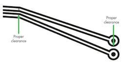
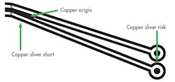
Slivers are a manufacturing failure that are best managed through proper board design (Fig. 1). To understand slivers, first we need to review the chemical etch process. The intent of the chemical etch process is to dissolve away the unwanted copper. But if there are extremely long, thin, sliver-like features to be etched away, these features can sometimes detach as chunks before they fully dissolve. The sliver chunks then float around in the chemical bath, where they might potentially land on another board randomly.
Equally risky is when the sliver is intended to stay attached to the board. If the sliver is narrow enough, the acid baths may etch away just enough copper underneath to partially detach the sliver. Now the sliver is flopping around, attached to the board like a flag. Invariably, it flips over onto your own board, and shorts out other traces.
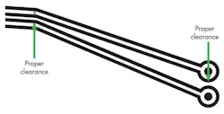
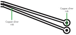
So where do you look for potential slivers and how do you avoid them? When laying out your PCB, it is best to avoid leaving very narrow areas of copper (Fig. 2). Such areas are usually caused by filled planes where trace and pad clearances intersect (Fig. 3). Keep the minimum width of copper areas above your manufacturer’s minimum and your design should be fine. A pretty standard minimum width for etching is 0.006 in.
6. Pay Attention to the DRCs
Whereas setting up the autorouter is often very specific to the design function, the Design Rule Checker is typically organized to capture a fabricator’s design constraints. While still tedious, it’s generally not quite as bad as the autorouter. Most design teams eventually create a set of design rules that aim to: standardize the bare board build costs and maximize yields; and make assembly, inspection, and test as consistent as possible. Beyond the design benefits, these design rules—by keeping designs within pre-defined fabrication limits—can also help create more consistency in the purchasing department as well. Pricing for the manufacture of the board is consistent, and purchasing can often reduce the number of specialized PCB manufacturing agreements that need maintaining.
To help with all this, many PCB design tools have a built-in DRC checker (some tools call them “constraint managers”) that will flag design rule violations for you interactively as you’re editing. Once you’ve set up the DRC rules for your fabricator of choice, get ready to take the errors seriously. DRC tools are, by design, conservative. They’ll err toward reporting a possible error, and let you decide. It can be tedious to sift through several hundred “possible” problems. Do it anyway. Somewhere deep in that list just might be the reason your first spin is destined to fail. Besides, if your design is triggering a lot of possible errors, you might want to take that as a hint that your trace placement needs some improvement.
Dave Baker, Sunstone Circuits, a PCB designer with over 20 years of design experience offers this advice. “Take time to understand and correctly set up the constraint system of your layout tool. Take the time to review all levels of your constraints. Constraint tools can be powerful and flexible, but also confusing and dangerous. Incorrect constraints can easily lead to defective or unbuildable boards. Errors in constraint setup can effectively limit or disable DRC checks. This can create a situation in which every DRC passes and yet the board is still unbuildable or non-functional. I’ve seen this happen before. The team is all happy because the board passes DRC and yet the first articles literally go up in smoke on the test bench. Tracing the failure took the team back to the CAD tool’s constraint manager. The constraint manager does not have a design conscience; it will let you do anything, no matter how bad.”
At Sunstone Circuits, for example, it’s an almost daily occurrence to receive a quote request for a board design that we could easily build, except for a critical area in which design tolerances and clearances were compressed dramatically. This situation puts the PCB fabs, such as Sunstone, in the position of delivering the bad news: either we can’t build the board at all because of the tolerances that are beyond our capabilities, or we can build the boards but at an increased price and at a riskier yield. These customers would have benefited from designing with a specific manufacturer in mind.
Baker adds, “If your layout software allows you to waive the DRC violations, then use that feature with caution. It is so easy to temporarily waive DRCs, meaning to get back to them later, and then forget them. Remember to review all waived DRC errors prior to sending your design for fabrication.”
Bob Tise, veteran PCB designer currently on staff with Sunstone Circuits, offers a counterpoint. “You could also just resist the temptation to waive DRCs altogether and just follow the rules you set up in the first place.”
7. Know The Fab You’re Using
After discussing DRC setup, this tip is almost—but not quite—redundant. Besides helping you set up the DRCs correctly, knowing which fab you’ll be sending your board also allows you some additional pre-fab help. A good fab will give you pre-order help and suggestions on how to approach your design to reduce design spins, reduce the number of issues you end up debugging on the bench, and increase your board yields overall.
On the blog onmyphd, Hugo, a PhD student at Carnegie-Mellon University, has this to say about knowing your manufacturer:
"Each manufacturer has its own specifications, such as minimum trace width, spacing, number of layers, etc. Before starting design, you should consider what you need and find a manufacturer that meets your requirements. Your requirements also include the grade of materials of the PCB. There are grades ranging from FR-1 (paper-phenolic mixture) up to FR-5 (glass cloth and epoxy). Most PCB prototyping manufacturers use the FR-4, but FR–2 is used in high-volume consumer applications. The type of material affects the circuit board’s strength, durability, moisture absorption, and flame resistance (FR)."
Understanding the processes that go into the manufacture of a printed circuit board will help you make better design decisions, as will knowing which processes and methods will be employed by your manufacturer. Set up a visit to your preferred supplier and walk through the processes; you might be amazed. And make use of DFM tools prior to submitting your design for fabrication.
Wrapping It Up
When you stay mindful of these essential skills and techniques, you’re well on your way to quick, reliable, professional-quality PCBs for your project. Understand the manufacturing processes; use DRCs and DFM to help you catch inadvertent design features that could increase your fab costs and/or decrease your yields. Then plan your component placement carefully to help eliminate the need for expensive design features. Make judicious use of all the design tools offered by your CAD tool, including autoplace and autoroute, but be patient and thorough about autorouter setup if you’re serious about autorouting successfully.
Don’t trust the autorouter to do anything more than place routes; adjust trace sizes by hand if necessary to ensure appropriate current flow for your design. And by all means, do trust the rat’s-nest lines. Until those are 100% gone, you have at least one open in your circuit.
Looking for parts? Go to SourceESB.
This file type includes high resolution graphics and schematics when applicable.


