Choose the Right Storage, Display Interfaces for Low-Power Mobile SoCs
This file type includes high resolution graphics and schematics when applicable.
Consumers today demand ultra-high-definition (UHD) display for 4K resolution in large-panel mobile devices and quad-HD (QHD) resolution in smartphones. To meet these needs while squeezing more functionality into a smaller package plus delivering low power and cost, designers must scrutinize every aspect of their mobile system-on-chips (SoCs)—not the least of which is selecting the right storage and display interfaces. Such interfaces must be able to support the higher transmission speeds required to store, read, and display the high-resolution content streams downloaded to the device via Wi-Fi or via radio transmissions, or captured by the image sensor.
Designers must consider several factors when selecting display and storage interfaces for their mobile SoCs, including the capabilities needed to support UHD display use-cases and high-throughput storage devices. In addition, they must address common power and performance challenges associated with implementing the required functions and features.
Meeting the Ultra-High-Definition Display Requirement
Consumers expect the same UHD viewing experience on their mobile devices as they do on their high-definition televisions. Today, more video content is viewed on mobile devices, demanding more networking support for the increased data traffic at faster speeds. Support for high-speed data networks like Long-Term Evolution (LTE) is now a key requirement. Consequently, mobile SoC designers must find a way to meet consumer demands by developing products that support super-fast networks and UHD displays while enabling longer battery life and maintaining reasonable bill-of-materials cost.
Higher-resolution content increases cost and power consumption. And such content requires more bandwidth to enable a better viewing experience. Higher costs stem from two factors:
• The design implementation is more complex, which requires costly SoCs and devices with sophisticated features.
• Key SoC design components must be redesigned and proven before production. At advanced process nodes, this becomes very costly and puts the return on investment (ROI) in question.
To enable high-resolution displays, increased video data throughput must be managed while reducing power consumption and electromagnetic interference (EMI). As more large-display mobile devices start to support 4K and higher-resolution formats, additional bandwidth is needed to handle the increased data throughput over the display interface. Consequently, designers must incorporate a high-speed physical layer (PHY) that supports greater bandwidth with more lanes and faster speeds (Table 1).
VESA Display Stream Compression for UHD
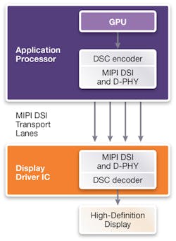
The Video Electronics Standards Association (VESA), in liaison with the MIPI Alliance Display Work Group, has developed the Display Stream Compression (DSC) Standard for interoperable, real-time, visually lossless compression over display interfaces. Implementing the DSC standard in conjunction with the MIPI DSI and D-PHY standards in a mobile-display SoC design helps compress the video data stream. As a result, transmission bandwidth over the display stream interface decreased threefold.
Furthermore, implementation of DSC dramatically reduced power consumption, resulting in longer battery life. And by being visually lossless, a viewer under normal conditions doesn’t see a difference between compressed video data and uncompressed video data on their device display, providing real-time, low display-latency compression and transmission. Other benefits include less EMI enabled by reduced signal switching, lower system cost due to fewer pins, and smaller frame buffers.
The ability to reuse components such as the MIPI D-PHY lowers the risks associated with architectural redesign, which also saves system and design costs. Perhaps best of all, the VESA DSC standard is highly interoperable with today’s display interfaces (Fig. 1).
Tables 2 and 3 show the number of lanes required when DSC encoding is used for different compression rates.
Selecting the Optimal Mobile Storage Interface
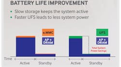
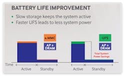
JEDEC Universal Flash Storage (UFS) is becoming a widely used standard in today’s high-end mobile device applications. The UFS storage solution offers high performance, reduces power, and, more importantly, improves the user experience. Users can enjoy 30% better response time for application loading and application switching, and achieve a 15% reduction in power compared to non-UFS mainstream mobile storage solutions. Higher transmission (burst) rates allow the design to switch to low-power mode sooner, resulting in a power reduction of approximately 15% compared to previous embedded storage standards (Fig. 2).
Because it significantly improves the user experience, the UFS storage solution is ideal for high-end mobile applications employing high-definition displays. However, other mobile storage solutions for mainstream mobile devices are worth considering. For example, the JEDEC Embedded MultiMediaCard (eMMC) standard consists of three components—the eMMC interface, flash memory, and flash-memory controller. The components are offered in a standard ball-grid-array (BGA) package similar to the UFS embedded storage device.
Both UFS and eMMC use a discrete controller to hide the complexity of managing the flash memory; hence, SoC designers benefit from the simplified flash-memory interface design and qualification process that results in reduced time to market. Also, the SoC design is future-proofed against the frequent changes in NAND-flash component supply, and designers can take advantage of the faster and less-costly UFS and eMMC devices as they become available.
Conclusion
Mobile SoC designers need the optimal display interface to enable UHD displays while reducing power and cost. The VESA DSC is an ideal standard to implement in a display interface solution in conjunction with the MIPI DSI and D-PHY specifications. Such a solution allows for compressed video-data transmission bandwidth while consuming lower power and offering the same visual experience as an uncompressed video-data transmission to an external display. The same design implementation (DSI protocol and D-PHY) can be used in a DSC implementation to reduce design risk and cost.
Mobile storage interface solutions implement eMMC and UFS standards, each providing its own unique benefits. While eMMC and SD standards are commonly supported in these solutions, the UFS option offers lower total system power and improves the user experience. UFS and eMMC standards complement each other, but they each target different price points, performance, and capabilities to address the large spectrum of mobile applications.
References:
Synopsys DesignWare MIPI IP


