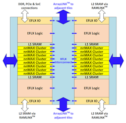
Flex Logix’s nnMax machine-learning (ML) inference engine technology, originally developed for embedded FPGAs (eFPGAs), will now be available in the InferX X1 coprocessor (Fig. 1). The nnMax tiles have been enhanced to implement Winograd calculations that improve performance and accuracy. The enhanced eFPGA version is also available.
1. Flex Logix’s nnMAX 1K inference tile delivers INT8 Winograd acceleration that improves accuracy while reducing the necessary computations.
The InferX X1 chip includes multiple nnMax clusters. It can deliver higher performance and throughput for neural-network batch sizes of one, which is typical for embedded edge IoT devices. The chips handle real-time object recognition by leveraging the YOLOv3 model at 11.4 frames/s using 2-Mpixel images with a batch size of one. This is accomplished with only a single DRAM. Performance scales linearly with image size; thus, the frame rate doubles to 22.8 frames/s for a 1-Mpixel image size.
Each nnMax tile has 1024, 1.067-GHz nnMAX DSP MACs. The chip also includes embedded RAM optimized for deep-neural-network (DNN) weight storage. The Winograd acceleration for INT8 layers delivers a 2.25X performance gain. The system transforms the 3-by-3 convolution to a 4-by-4 with dynamic translation of weights to 12 bits. The support also handles input and output translation on-the-fly, minimizing the loading of weights within the system.
The InferX X1 is designed for inference only. Other platforms, like NVIDIA’s GPGPUs, are better for training models. Flex Logix’s compiler takes these models and optimizes them for running on the coprocessor. The chip supports INT8, INT16, and BFLOAT16. Multiple models can be processed in parallel. The compiler supports standard machine-learning platform formats like TensorFlow and ONNX.
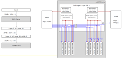
The compiler and chip can also optimize model processing by combining the number of layers that are processed simultaneously. Typically, layers are processed sequentially with buffers storing intermediate results (Fig. 2). This can get costly in terms of memory and latency, since larger buffers need to be stored in DRAM, which has a slower access time.
2. A system like InferX typically processes neural-network layers one at a time, buffering the intermediate results, but this can be costly in time and storage (click on image for enlarged version).
Flex Logix’s solution is to combine the processing of layers so that the intermediate values can be stored in on-chip memory (Fig. 3). Clusters are allocated to handling different layers to minimize weight loading and storing of intermediate values. The system still requires the same number of calculations to be performed. However, the approach has each group of files handling a smaller number of calculations at the same time, with a larger number of iterations to make up the difference. This significantly boosts performance as well as lowers power requirements compared to buffering or using competing hardware.
3. Combining two or more layers in a single computational step can eliminate the need for large buffers to handle intermediate values (click on image to enlarge).
The InferX X1 is built using TSMC 16FFC technology. It delivers 8.5 TOPS and has 4095 MACs overall with 8 Mbytes of SRAM. The InferX X1 chips will be available later this year along with a pair of PCI Express (PCIe) cards. One has a single InferX X1 chip with a single LPDDR DRAM while the other has a pair of chips and DRAM. The half-height, half-width cards are designed for embedded servers.
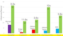
The type TDP for the PCIe cards running the YOLOv3 model is 9.6 W. Lighter-weight models require less power. For example, ResNet-50 uses only 2.2 W. The chip has very favorable inference times compared to other ML hardware running the same models with a batch size of one (Fig. 4).
4. InferX X1 delivers higher inference speeds with a batch size of one compared to the competition.


