Technology Claims to Find Sweet Spot Between NAND and DRAM
Intel and Micron Technology have introduced a new kind of memory chip to address the the explosive growth of digital data.
The technology, called 3D XPoint (pronounced “cross point”) is being described as both fast and nonvolatile, meaning that it can serve as either system memory or digital storage. The result, according to Micron's chief executive Mark Durcan, is the first new memory category to be released since NAND Flash in 1989.
The new technology is a kind of hybrid between dynamic random-access memory (DRAM) and solid-state NAND Flash drives. “It’s up to 1000 times quicker, and writeable in small amounts, so it can be used as memory,” said Robert Crooke, the senior vice president and general manager of Intel’s Non-Volatile Memory Solutions Group, at a press conference this week.
“But it’s also nonvolatile, so it can be used as storage,” he added. DRAM technology is capable of accessing memory faster than 3D XPoint. Because DRAM is volatile, however, it needs a constant supply of power to save data. In contrast, solid-state NAND Flash is nonvolatile but significantly slower than DRAM and 3D XPoint.
For its part, 3D XPoint technology is built with thin columns of densely packed memory cells stacked in a three-dimensional crosshatch pattern. The cells intersect across word lines and bit lines, allowing them to be written and accessed individually. According to Micron and Intel, this results in about 1000 times lower latency than NAND Flash, which is forced to erase entire blocks of cells in order to rewrite data. The 3D technology can be stacked between eight and ten times the density of DRAM chips and will be significantly more durable than NAND Flash, Crooke said.
The memory cells are written through “bulk material property change.” By varying the amount of voltage sent to each selector, the cell changes its physical characteristics to have either high or low electrical resistance, programming the cell to be a zero or a one. This approach removes the need for transistors in the memory cell – one of the main reasons DRAM technology is so expensive. The cost-per-bit for the new technology, Crooke said, should be somewhere between NAND and DRAM.
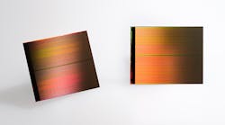
Intel and Micron did not reveal much of the underlying architecture behind 3D XPoint. But both have stated that the technology is targeting programs that have to evaluate large data sets, like video games, image recognition, and the analysis of genomes in medical research. 3D XPoint wafers are currently running in production lines at a joint Micron-Intel facility in Utah. Intel and Micron unveiled a 128-Gigabit wafer at a press conference.
After reporters were invited to the press conference earlier in the week, there were rumors that Micron would discuss the recent $23 billion bid from China's Tsinghua Unigroup to buy the Idaho-based chipmaker. These rumors were fueled by Intel's 15% stake in the state-backed Tsinghua.
The offer quietly fell into the background after the 3D XPoint announcement. A release date for the technology has not been announced.

