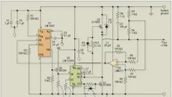
Negative Supply Uses Positive Hysteretic Regulator
Frequently, the use of a hysteretic regulator is preferred because of its simplicity of use and wide input-voltage range. For example, National Semiconductor's LM5007 is a constant-on-time variation of the hysteretic topology, but offers a nearly constant frequency of operation. Most of the standard hysteretic regulators are set up for positive-buck applications, with little support for negative-output requirements.
The circuit in the figure illustrates the implementation of a negative buck constant-on-time IC. The circuit is built around the LM5007 constant-on-time regulator, without much additional complication over the positive-buck implementation, for which the LM5007 was designed. The switching output of this device is configured to source current directly into the inductor, which is standard for a positive-buck implementation. In this application, transistor Q3 inverts the drive output of U1. Therefore, when this output is high, Q1 now sinks inductor current to -VIN. Q2 functions as a synchronous rectifier, using the high-side drive of U3. Q2 is bypassed by a Schottky diode D3, pointing toward system ground.
A hysteretic regulator depends on the ripple voltage on the output (caused in this circuit by the ripple current through R6 and the ESR of C2) to trigger the next on-time cycle. In the case of a negative regulator, this ripple is referenced to -VOUT, but the LM5007 is referenced to -VIN. To solve this problem, the differential amplifier U2 functions as a unity-gain level shifter, effectively moving the ripple reference to -VIN. Resistor divider R3/R4 must divide down the average output voltage to -2.5 V, whose absolute value is the trigger threshold for U1. Two things are important regarding U2. First, the gain must be unity, since the dc level of the R3/R4 divider is level shifted along with the ripple component. Second, one must be careful to get the peaks and valleys of the ripple in the proper inversion, otherwise what should be a peak at the trigger input could appear as a valley.
There must be at least 50 mV of ripple on the 2.5-V signal applied to the FB pin of U1 to ensure reliable triggering. The purpose of R6 is to add resistance to the ESR of C2, which increases the ripple component on the output. R6 is listed in the schematic as 1 Ω, but this should be adjusted to tune in the required ripple voltage. The LM5007 datasheet includes some additional circuitry to allow operation at reduced ripple. Those techniques also apply to this negative converter implementation.
Since U1 is now driving a PMOS FET (Q3), whose source is tied to U1's VIN pin, instead of directly driving a power inductor, the bootstrap capacitor C4 on the BST pin is not required. However, it is retained to act as a noise filter.
The value of -VIN in this circuit is -20 Vdc, although U1 is actually rated for an input voltage up to a magnitude of 80 V. For applications where the magnitude of -VIN exceeds 20 Vdc, U2 and the other components must also be rated for 80 V.
