FAQs: Pulse-Width Modulation (PWM) and Switch-Mode Converters
What you'll learn:
- How pulse-width modulation (PWM) works with switch-mode converters.
- How PWM can be used in different power-switching applications.
Table of Contents
- What is the purpose of pulse-width modulation (PWM)?
- Why do PWM circuits need slope compensation?
- What function does the UVLO circuit perform?
- What output configurations are available with PWM controllers?
- What is the purpose of current sensing?
- Is the PWM frequency variable?
- Can the PWM frequency be synchronized to an external clock?
- What is the purpose of the soft-start circuit?
- What are some of the current pulse-width-modulator ICs?
What is the purpose of pulse-width modulation?
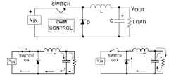
Switch-mode converters employ a power semiconductor switch (usually a MOSFET) to drive a magnetic element (transformer or inductor) whose rectified output produces a dc voltage. Efficiencies exceeding 90% are common, about twice that of a linear regulator.
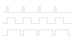
A switch-mode converter varies its dc output current in response to load changes. One widely used approach is pulse-width modulation (PWM) that controls the power switch output power by varying its ON and OFF times. The ratio of ON time to the switching period time is the duty cycle. Figure 1 shows three different variations of the PWM duty cycle: 10%, 50%, and 90%. The duty cycle and power handling rarely have anything to do with each other. Instead, the duty cycle is adjusted to regulate the output voltage.
What is the configuration of a PWM circuit?
Figure 2 shows a simplified PWM controller employed in a switch-mode converter. In operation, a fraction of the dc output voltage feeds back to the error amplifier, which causes the comparator to control the PWM ON and OFF times. If the power MOSFET’s filtered output changes, the feedback adjusts the duty cycle to maintain the output voltage at the desired level.
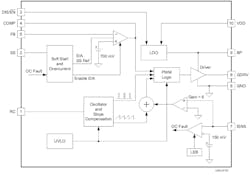
To generate the PWM signal, the error amplifier accepts the feedback signal input and a stable voltage reference to produce a output related to the difference of the two inputs. The comparator compares the error amplifier’s output voltage with the ramp (sawtooth) from the oscillator, producing a modulated pulse width. The comparator output is applied to the switching logic, whose output goes to the output driver for the external power MOSFET. The switching logic provides the capability to enable or disable the PWM signal applied to the power MOSFET.
Why do PWM circuits need slope compensation?
PWM duty cycles above 50% require a compensating ramp, called slope compensation, to avoid instability. Higher duty cycles require even greater slope compensation. That is, if the PWM switch is turned on for more than 50% of the switching period, slope compensation must be used to keep the system stable. With traditional slope compensation, the switching converter may become unstable for duty cycles approaching 100%, so a special slope compensation must be employed. Figure 3 shows a PWM controller that employs slope compensation.
What function does the UVLO circuit perform?
The undervoltage-lockout (UVLO) circuit sets the operational dc input voltage range of the PWM controller. There are two UVLO thresholds. When the UVLO turn-on threshold is exceeded, the PWM controller turns ON. If dc input voltage falls below the UVLO’s turn-off threshold, the PWM controller turns off.
What output configurations are available with PWM controllers?
PWM controllers may have single-ended or dual outputs. Dual output types are intended for either for push-pull, bridge, or synchronous-rectifier MOSFETs. In these configurations, the PWM controller must either accurately set the two outputs' dead time or prevent their overlap. If both outputs were allowed to be ON simultaneously, it would increase power dissipation and EMI. Some PWM controllers include special circuits to control dead time or overlap.
What is the purpose of current sensing?
Most PWM controller ICs provide current-limiting protection by sensing the output current. If the current-sense input exceeds a specific threshold, it terminates the present cycle (cycle-by-cycle current limit).
Circuit layout is critical when using a current-sense resistor, which must be a low inductance type. Locate it and the current-sense filter capacitor is very close to and connected directly to the PWM IC pin. Also, all of the noise-sensitive, low-power ground connections should be connected together near the IC ground and a single connection should be made to the power ground (sense-resistor ground point).
Is the PWM frequency variable?
In most PWM controller ICs, a single external resistor or capacitor sets the oscillator frequency. To set a desired oscillator frequency, use the equation in the controller datasheet to calculate the resistor value.
Can the PWM frequency be synchronized to an external clock?
Some PWM converters include the ability to synchronize the oscillator to an external clock with a frequency that's either higher or lower than the frequency of the internal oscillator. If there's no requirement for synchronization, connect the sync pin to ground to prevent noise interference.
What is the purpose of the soft-start circuit?
The soft-start feature allows the power converter to gradually reach the initial steady-state operating point, thus reducing startup stresses and surges. In most PWM ICs, an external capacitor establishes the soft-start time.
What are some of the current pulse-width-modulator ICs?
Using PWMs in a high-speed pulse-width modulator
Microchip Technology’s MCP1631 and MCP1631V are high-speed analog PWMs. When combined with a microcontroller, the MCP1631/MCP1631V can control the power system duty cycle, providing output voltage or current regulation. The microcontroller can be used to adjust output voltage or current, switching frequency, and maximum duty cycle while providing additional features, making the power system more intelligent, robust, and adaptable.
The MCP1631 (current-mode control) and MCP1631V (voltage-mode control) contain the PWM, MOSFET driver, current-sense amplifier, voltage-sense amplifier, and overvoltage comparator. These ICs operate with a 3.0- to 5.5-V input. Additional features include shutdown, UVLO, and overtemperature protection.
For applications that operate from a high-voltage input, the MCP1631HV and MCP1631VHV can operate directly from a +3.5- to +16-V input. For these applications, an additional low-dropout +5- or +3.3-V regulated output is available and can provide current up to 250 mA to power a microcontroller and auxiliary circuits
The internal PWM of the MCP1631/MCP1631V consists of an error amplifier, high-speed comparator, and latch. The output of the amplifier is compared with either the MCP1631 CS (primary current-sense input) or the MCP1631V VRAMP (voltage-mode ramp input) of the high-speed comparator. When the CS or VRAMP signal reach the level of the error amplifier output, the on cycle is terminated and the external switch is latched off until the beginning of the next cycle.
Among typical applications for the MCP1631/MCP1631V include programmable switch-mode battery chargers capable of charging multiple chemistries, like Li-ion, NiMH, NiCd, and Pb-acid configured as single or multiple cells. By combining with a small microcontroller, intelligent LED lighting designs and programmable SEPIC topology voltage and current sources can also be developed.
The MCP1631/MCP1631V inputs can be attached to the I/O pins of a microcontroller for design flexibility. Additional features integrated into the MCP1631HV/MCP1631VHV provide signal-conditioning and protection features for battery charger or constant-current source applications.
PWMs and current-mode boost controllers
Shown in Figure 3 is Texas Instruments' TPS40210 and TPS40211 wide-input-voltage (4.5 to 52 V), non-synchronous boost controllers. They're suitable for topologies that require a grounded source N-channel FET, including boost, flyback, SEPIC, and various LED-driver applications.
Device features include programmable soft-start, overcurrent protection with automatic retry, and programmable oscillator frequency. Current-mode control provides improved transient response and simplified loop compensation. The main difference between the two parts is the reference voltage to which the error amplifier regulates the FB pin.
A resistor and capacitor connected to the RC pin determine the oscillator frequency. The capacitor charges to about VDD/20 by current flowing through the resistor and is then discharged by a transistor internal to the TPS40210. You can synchronize the TPS40210 and TPS40211 to an external clock whose frequency must be higher than the converter’s free-running frequency.
The TPS40210 and TPS40211 are current-mode controllers and use a resistor in series with the source terminal power FET to sense current for both the current-mode control and overcurrent protection. The current-sense resistor serves as both a current limiter and current-mode control sense, so it must be selected based on both the stability (current-mode control limitation) and current limit (device limitation).
Standard boost converters have no method to limit current from the input to the output in the event of an output short circuit. If protection from this type of event is desired, it's necessary to use some secondary protection scheme.
A characteristic of peak current-mode control is a condition where the current control loop becomes unstable. The voltage loop maintains regulation, but the output ripple voltage increases and oscillates at one-half the switching frequency.
The remedy for this condition is to apply a compensating ramp from the oscillator to the signal going to the pulse width modulator. In the TPS40210/11, the oscillator ramp is applied in a fixed amount to the pulse width modulator. To ensure that the converter doesn't enter into sub-harmonic instability, the slope of the compensating ramp signal must be at least half of the down slope of the current ramp signal.
Because the compensating ramp is fixed, it places a constraint on the selection of the current-sense resistor. The slope-compensation ramp must be at least half, and preferably equal, to the down slope of the current-sense waveform seen at the pulse-width modulator. A maximum value is placed on the current-sense resistor when operating in continuous mode at 50% duty cycle or greater.
For design purposes, some margin should be applied to the actual value of the current-sense resistor. As a starting point, the actual resistor chosen should be 80% or less than the resistor value that makes the slope-compensation ramp equal to one half of the current ramp down slope.
Synchronous buck PWM DC-DC controller
The Analog Devices ADP1828 is a versatile and synchronous PWM voltage-mode buck controller. It drives an all N-channel power stage to regulate an output voltage as low as 0.6 V to 85% of the input voltage and is sized to handle large MOSFETs for point-of-load regulators.
The ADP1828 is well-suited for a wide range of high power applications, such as DSP and processor core I/O power, and general-purpose power in telecommunications, medical imaging, PC, gaming, and industrial applications.
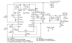
Shown in Figure 4, the ADP1828 operates from input bias voltages of 3 to 18 V with an internal LDO that generates a 5-V output for input bias voltages greater than 5.5 V. The control circuits, gate drivers, and the external boost capacitor operate from the LDO output for an input between 5.5 and 18 V.
PV powers the low-side MOSFET gate drive (DL), and IN powers the internal control circuitry. Bypass PV to PGND with a 1-μF or greater capacitor, and bypass IN to GND with a 0.1-μF or greater capacitor. Bypass the power input to PGND with a suitably large capacitor.
The switching frequency can also be synchronized to an external clock up to 2× the part’s nominal oscillator frequency. The clock output can be used to synchronize additional ADP1828s (or the ADP1829 controllers), thus eliminating the need for an external clock source.
The ADP1828 includes soft-start protection to limit any inrush current from the input supply during startup, reverse-current protection during soft start for a pre-charged output, as well as an adjustable lossless current-limit scheme utilizing external MOSFET RDS(ON) sensing.
For applications requiring power-supply sequencing, the ADP1828 provides a tracking input that enables the output voltage to track during startup, shutdown, and faults. The additional supervisory and control features include thermal overload, UVLO, and power good.
The ADP1828 operates over the −40 to +125°C junction temperature range and is available in a 20-lead QSOP
Original publish date: April 10, 2009
Updated: July 25, 2024


