Hysteretic-Mode Converters Demystified, Part 2: Voltage and Current Mode Control
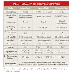
To compare operating modes, there is one voltage-mode (VM) device on its evaluation module (EVM), IC-VM; one current-mode (CM) device on its EVMs in two different configurations (IC-CM and IC-CM2); and one hysteretic-mode device on its EVM, IC-HM. Table 1 summarizes the specifications of these four EVMs.
Large-Signal Load-Transient Response
The first major performance item to review is large-signal load-transient response performance. Here, a large-signal phrase is used in contrast to a small-signal. A small-signal transient literally uses small-signal perturbation and is compatible with many ac performance measurements such as Bode plots and output impedance. A large-signal transient gives big signal perturbation where the bias points of the circuit/system change widely. When bias points move, it is no longer in a scope of ac measurements.
Practically speaking, almost all load-transient curves on a step-down converter data sheet are large-signal transients. No doubt, a large-signal transient is a major tool to gauge regulator undershoot and overshoot voltage performance.
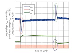
Figure 1 is an example waveform taken for large-signal load transient analysis comparing these waveform combinations:
- Input voltage: 5 V and 12 V
- Load-transient amplitude: 500 mA to 5A and 50 mA to 500 mA
- Output capacitor: default setting in Table 1 plus 1000 µF
In Fig. 1, notice the undershoot event at the timing of the output current rise (red circle), and an overshoot event when the output current falls (green circle).
These measurements use around 30 ns/A of a very fast transient. Because of this fast transient, the output-current waveform shows a severe spike at its falling edge (blue circle) in Fig. 1.
Base Comparison Result
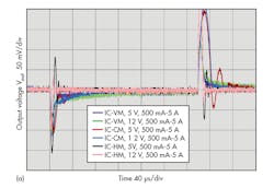
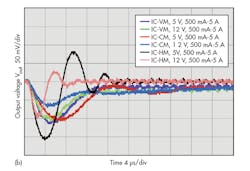
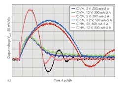
Figures 2a-c compare IC-VM, IC-CM and IC-HM with a transient from 500 mA to 5 A, then back to 500 mA at 5V and 12V input voltage settings. Figures 2b and 2c zoom in on the plot shown in Fig. 2a.
Undershoot
Undershoot behavior (Fig. 2b) expresses how fast the control circuitry can respond to its output current change. At the bottom of the first undershoot peak, the regulator drives its inductor current more than the load current, where excess current starts charging back the output capacitor while delivering load current (Figs. 6 and 7 in part 1). In Fig. 2(b), IC-HM appears to have the fastest response by hitting the undershoot bottom faster than either IC-VM or IC-CM.
During an undershoot event, a drop-in amplitude is a strong function of output capacitance, where the bigger the COUT, the smaller the voltage drop. In Table 1, IC-HM has less than half of the output capacitance of IC-VM and less than a quarter of the capacitance of IC-CM. Still, IC-HM shows a level of voltage drop similar to IC-VM and IC-CM. The reason is that a hysteretic-mode converter can react with a very small circuit delay in response to any load change. With a hysteretic-mode converter, the response is almost the same as a physical limitation in how fast the inductor current can increase. In the case of VM and CM converters, these converters work in two steps. The first is to change their control signal, which is an output of their error amplifiers. The second is that the control signal changes output pulse duty or density. In general, such pulse duty or density change is much slower than the way hysteretic-mode converters react.
Similar to Fig. 2(c), IC-VM shows no ringing by input voltage or output current. IC-CM and IC-HM shows some ringing, where Fig. 2(b) shows the phase margin at a 5A output.
Overshoot
Regarding overshoot behavior (Fig. 2c), the first peak of each curve is determined by the inductor and the output capacitor on each board, not by the converter IC. When the output current suddenly falls down to a small value, energy stored by the inductor has no path, but charges the output capacitor. Looking at Table 1, the IC-HM has the smallest output capacitance; thus, the IC-HM shows the biggest overshoot. On the other hand, the IC-VM has the smallest inductance; thus the IC-VM shows the smallest undershoot.
As for the overshoot, the behavior after the first peak that comes back to its target output voltage indicates the phase margin of each device. IC-VM shows no ringing (no second peak), but IC-CM and IC-HM do show some ringing peaks. This means that IC-VM has better phase margin against IC-CM or IC-HM. Fig. 2(c) shows phase margin at a 500-mA output current. Part 3 of this series will review the loop stability of each board in detail.
Voltage, Current, and Hysteric-Mode Insights
Voltage-Mode Insights
In Fig. 2(b), the IC-VM waveforms show little difference because of the voltage feed-forward configuration. A simple simulation model (results not shown here) confirms that this configuration of VM devices completely keeps the same response of its control signal, VC (output of its error amplifier) regardless of input voltage or output-current difference. The same VC response brings the same output-voltage response.
When reusing one design for multiple power-rails, a VM device can be a good option. Even though a Type III compensation design takes time, once the first design is done, it can work a wider range of input voltage with a similar response behavior.
Current-Mode Insights
One interesting observation from Fig. 2(b) is that the IC-CM waveform with 5-V input shows ringing during its undershoot condition before the output voltage reaches the target value. This ringing is caused by its inner current loop. With a single-loop control like IC-VM or IC-HM, ringing always happens when the output voltage comes back to its target value.
The inner-current-loop ringing happens like this. As undershoot starts, VC demands a rapid increase of inductor current. Since IC-CM is a peak-current mode device, the device remains on until the inductor current hits a new VC target. Because inductor current slew rate is a function of input voltage (shown in Equation 1), apparently, a 5V input-voltage curve takes more time to hit a new VC than a 12V input voltage curve:
As it takes longer to hit the target VC, the error amplifier actually drives VC further up as the output voltage drops more. This results in too much inductor current until it hits VC in the undershoot event; this high VC condition causes ringing.
Even though 5V shows ringing and 12V shows smooth undershoot, the compensation circuit at its error amplifier is the same. With a simple and ideal simulation model (results not shown here), both a 5V undershoot curve and a 12V curve follow the same target trace.
Hysteretic-Mode Insights
In Fig. 2(b), the IC-HM waveform with 5V input shows a ringing. Unlike IC-CM case, this IC-HM ringing is triggered when the output voltage comes back to the target.
The severe ringing at a 5V input condition is similar to the IC-CM case shown by Equation 1: that a smaller input voltage limits inductor-current change. Because of the slow inductor current increase, the output capacitor discharge is more than a 12V input condition. The output-voltage comparator keeps driving its output pulse at the maximum frequency until the output voltage comes back to the target. When the output voltage hits the target, inductor current is actually too high (compared with the 12V input case) and that high inductor current overcharges the output capacitor.
Output Capacitance and Current Difference
Output Capacitance Difference
In an ideal situation, do not change an output-capacitor value after finalizing a loop-compensation design because a loop-stability design is a direct function of the output-capacitor value. In a real-world application, the output-capacitor value tends to increase. For example, your final power regulator block gets combined with a digital processor block, which has a huge amount of bypass capacitors. Therefore, the 1000 µF output capacitor condition simulates an increased output capacitor scenario.
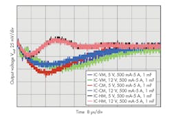
Figure 3 shows a comparison of a large-signal load transient from 500 mA to 5 A, then back to 500 mA at 5V and 12V input with a 1000 µF output capacitor on each board. To avoid repeating similar comments, Fig. 3 only shows undershoot events on each board.
With a 1000 µF output capacitor, all control modes show a slower response due to the lower cutoff frequency of the LC filter. Note that both X-axis and Y-axis scales of Fig. 3 are different from Fig. 2, which shows a bigger capacitor-suppress undershoot amount (as expected).
In Fig. 3, IC-HM shows significant improvement on the undershoot amount (amplitude) versus improvements on IC-VM and IC-CM.
Note that 1000 µF capacitors are solder-mounted on IC-CM and IC-HM, but the 1000 µF capacitor is wire-connected on IC-VM because the EVM has space limitations. With this wire, IC-VM waveforms show glitches just at the beginning of undershoot. These glitches are the result of wire inductance.
Output Current Difference
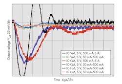
Figure 4 compares two different large-signal load transients:
1. From 500 mA to 5 A, then back to 500 mA.
2. From 50 mA to 500 mA, then back to 50 mA at a 5V input, showing only undershoot events.
Note that some waveforms show a switching ripple of around 2.5 cycles in one 4µs division of timescale, which is not ringing.
In Fig. 4, the IC-VM has good stability at a 50 to 500mA transient as well as a 500mA to 5A transient, where IC-CM and IC-HM exhibit ringing in both high- and low-current transients. These results are expected as the output current level does not change the transient response.
Duty (Pulse-Density) Change at Load Transient
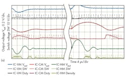
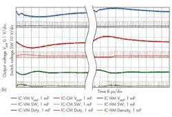
Figures 5(a-b) show the same large-signal load transients already reviewed in previous subsections, but plotted with a switch-node pulse and its average. A rolling average equation calculates a duty signal from the switch-node pulse density. Figure 5(a) uses the default output capacitor settings, and Fig. 5(b) has 1µF capacitance. Note that Figs. 5(a-b) have different time and voltage scales.
Comparing Figs. 5(a-b) confirms that:
- IC-VM and IC-CM are working with pulse-width modulation (PWM) control. IC-HM is changing the frequency of its constant ON pulse.
- IC-HM changes its frequency much faster than IC-VM, or IC-CM changes its duty. This is why IC-HM shows a faster transient response.
- With a bigger output capacitor, duty or pulse-density change is smaller; thus the transient response of all three control modes becomes slower. The IC-VM with 1000 µF has almost an invisible duty change.
- IC-HM has a pulse-density limit because of a minimum OFF time setting, where the minimum OFF time is preventing its inductor from saturated conditions. Still, IC-HM shows the fastest response among the three control modes.
Tweaking IC-CM Faster/Tweaking IC-HM with Smaller Undershoot
These large-signal load transient comparisons have revealed that IC-HM has the fastest response, but also the biggest overshoot and undershoot.
To make evaluation boards conditions closer, there will be two additional experiments here:
- Modify IC-CM to have faster response to the similar response level of IC-HM. This is IC-CM2. To make this happen, I redesigned IC-CM2’s loop compensation and increased its switching frequency (Table 1).
- Modifying IC-HM to have a 200-µF output capacitor, the same as IC-CM. Thanks to the internal ripple-injection design, there is no board change except for replacing the output capacitors. So this board is still called IC-HM, just with 200 µF.
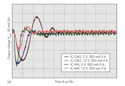
To match IC-HM’s speed, IC-CM2 has very fast switching frequency with a very stretched, wide control-loop bandwidth. Because of this setting, a ceramic-type capacitor won’t provide stable operation. As mentioned in part 1, the IC-CM2 board has the ultimate stability option: a tantalum capacitor for the stability. Because of the tantalum capacitor, equivalent series resistance (ESR) is very large, and overshoot and undershoot get worse.
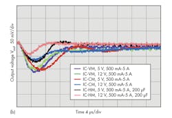
Figure 6(a) compares IC-CM2 and IC-HM while Fig. 6(b) compares IC-HM with 200 µF and IC-CM.
In Fig. 6(a), IC-HM waveforms have no change from Fig. 2(b). IC-CM2 is showing much faster transient response than IC-HM as expected at the cost of less stability. There are many CM converter devices in the market that can work at a megahertz order of switching frequency. But it is difficult to find a converter IC that can maintain its stability with a wide control bandwidth. It is not shown here, but IC-CM2 loses its stability at a lower output current, even though it uses a tantalum capacitor.
Using a higher switching frequency for IC-CM2 automatically reduces its conversion efficiency due to increasing switching and gate-drive loss. I will discuss conversion efficiency later in this document. Here, in contrast to a current-mode, the beauty of hysteretic-mode convers is its pulse-frequency modulation (PFM) operation where switching becomes faster only at a transient event. Note that changing frequency is not always a good thing as it increases noise concerns.
Figure 6(b) replaces the IC-HM waveforms from Fig. 2(b) with ones using the 200-µF output capacitor. IC-HM waveforms with 200-µF capacitors show excellent transient performance, smaller undershoot amplitude and a shorter undershoot period compared to IC-VM or IC-CM.
Line-Transient Response
In reviewing the line-transient response performance waveforms, the line-transient comparison uses these combinations of waveforms:
- Output current: 5 A, 1.5 A, 500 mA, 50 mA
- Line-transient amplitude: 5 V to 6 V and 12 V to 13 V
- Output capacitor: default setting from Table 3 pulse 1000 µF
To obtain a visible response at an output voltage, I set the line-transient amplitude to have a 1V step, which means this is a group of large-signal measurements. Unlike the large-signal load-transient analysis in the previous section, there are few observations to make from this line-transient analysis.
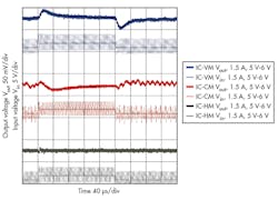
Figure 7 shows 5- to 6-V transient waveforms at a 1.5A output current, where you can clearly see the control-mode differences. For this analysis, the line-transient rate is around 1V/µs. Because a high-speed power amplifier makes the transients, there is a limit to how much capacitive load the amplifier can drive. Given this limitation, input capacitors of each board are reduced to 0.1 µF; that is why there is severe spike noise on the input-voltage waveforms in Fig. 7.
Figure 7 confirms that:
- IC-HM has the best line-transient response because of no duty (density) control, in the same way as in the large-signal load-transient section.
- IC-CM gets the second-best line-transient response performance, but there is not much significant difference from the last position of IC-VM. Both IC-VM and IC-CM show a 10-mV range scale of line-transient overshoot and undershoot.
- Not all waveforms are shown here, but IC-HM shows superior line-transient performance throughout all combinations taken for this analysis.
Power-Conversion Efficiency
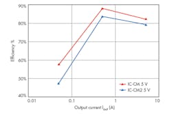
Let us briefly review power-conversion efficiency. Because it is not an apples-to-apples comparison, there is no point in making an absolute-value comparison of efficiency curves. Here, check the differences between IC-CM and IC-CM2 to see the impact of increasing switching frequency.
Figure 8 compares IC-CM and IC-CM2; these two boards have 633kHz and 1.2MHz switching frequencies, respectively. IC-CM2 clearly shows the effect of increasing gate-drive loss. Even though IC-CM2 can achieve a very fast transient response, this fast transient is at the cost of efficiency and also stability (as reviewed in the previous section).
Summarizing the transient response performance of each control mode:
Voltage-mode control:
- consistent response over a wide range of parameter changes
- relatively slower response than CM or HM
- less ringing compared with CM or HM
Current-mode control:
- response speed in the middle of VM and HM
- ringing caused by a current-loop
Hysteretic-mode control:
- faster response than VM or CM
- changing switching frequency at any transient event
- smallest ringing at same output capacitance conditions than VM or CM
- severe ringing when used with vender-recommended output capacitance value, which is usually smaller than recommended values for VM and CM
References
- Brian Cheng, Eric Lee, Brian Lynch and Robert Taylor. Choosing the Right Fixed Frequency Buck Regulator Control Strategy, 2014 Texas Instruments Power Supply Design Seminar (SLUP317).
- Brian Cheng, Eric Lee, Brian Lynch and Robert Taylor. Choosing the Right Variable Frequency Buck Regulator Control Strategy, 2014 Texas Instruments Power Supply Design Seminar (SLUP319).
- SW Lee, Demystifying Type II and Type III Compensators Using Op-Amp and OTA for DC/DC Converters, Texas Instruments Application Report (SLVA662), July 2014.
-
Everett Rogers, Understanding Buck Power Stage in Switchmode Power Supplies," Texas Instruments Application Report (SLVA057), March 1999
About the Author
Masashi Nogawa is a senior systems engineer for Texas Instruments’ Power Management group, where he is responsible for the SWIFT product line. Masashi received his bachelor’s and master’s degrees in electrical engineering from the University of Electro-Communications, Tokyo, and he holds six U.S. patents. Masashi can be reached at [email protected].
About the Author
Masashi Nogawa
Senior Systems Engineer
Voice Your Opinion!
To join the conversation, and become an exclusive member of Electronic Design, create an account today!

Leaders relevant to this article:
