Why More-Than-Moore Power Management Is Required to Keep Up With Exponential Growth in ICT Data Consumption
Significant gains in energy efficiency are required to keep up with the exponential growth in the data consumption of Information and Communications Technology (ICT) systems: end-user devices, networks, and data centers. Moore’s Law scaling (monolithic integration in silicon) is the historical technology driver, but it no longer achieves the required gains. Fortunately, a new power-management technology has emerged. It achieves More-than-Moore scaling by integrating different components and materials to increase functional diversity and parallelism. This technology can improve voltage regulator power density, response time and granularity by an order-of-magnitude to reduce the ICT system energy consumption by 30% or more. This paper explains why a Heterogeneously Integrated Power Stage (HIPS) enables power management scaling to keep up with the rising demands on data centers and network systems.
Exponential Growth in Data Consumption
The digital universe—the data we create and copy annually—will grow 10x, from 4.4 zettabytes to 44ZB, from 2013 to 2020. The forecast for 2020 compared to 2014 expects many more Internet users (3.9 billion versus 2.8 billion), more connected devices (24.4 billion versus 14.2 billion), faster average broadband speeds (42.5Mbps versus 20.3Mbps) and more video streaming (80% versus 67% of traffic). Most people will use a tablet or smartphone for all online activities by 2018. Mobile data traffic is increasing 10x from 3.3 exabytes per month in 2014 to 30.5EB/month in 2020. Many websites (e.g., Facebook) require an order of magnitude more power to build a web page than to deliver it.
ICT Energy Consumption
According to one study, ICT systems in 2012 consumed 920 terawatt-hours of power, which is 4.7% of global electricity consumption. That power requires the equivalent of 300 coal plants and emits 2 trillion pounds of CO2-equivalent greenhouse-gas emissions.
A second study forecasts that improvements in energy efficiency will slow the growth in ICT electricity consumption from the historical 6.7% per year to 3.8% per year due to the following:
• Each new generation of ICT systems and components is more energy[efficient. For example, improvements in optical components enable an order-of-magnitude increase in data rates of optical modules within roughly the same power envelope.
• Usage is shifting from energy-intensive TVs and conventional desktop PCs to energy-efficient smartphones, ultrathin notebooks, tablets, and fanless all-in-one desktop PCs. In 2011, the average annual electricity consumption was just 5.5 kilowatt-hours for smartphones and 16kWh for tablets, compared to 219kWh for PCs.
• Increasingly, networks and data centers will be optimized for energy efficiency rather than capacity. One example of an industry initiative is Greentouch, whose mission is to deliver the architecture, specifications, and roadmap to increase network energy efficiency by 1,000x compared to 2010 levels.
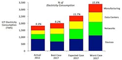
However, a third study estimates that ICT systems’ percentage of global electricity consumption was 9.3% in 2012 and will grow in 2017 to 9.2%, 11.7%, or 15.6% according to three different growth scenarios, as Fig. 25-1 shows. Data-center operating costs (OPEX) are beginning to exceed capital expenditures (CAPEX) in the total cost of ownership. As applications and data move into the cloud, energy consumption is shifting from client devices to networks and data-center infrastructure. This shift highlights the need to increase the energy efficiency of data centers and networks.
25-1. ICT Electricity Consumption Forecasts.
Moore’s Law Scaling
Moore’s Law (as revised by Gordon Moore in 1975) predicts that the number of transistors per chip can double every 24 months. Although the industry is now slipping behind this rapid pace, each new process-technology generation still provides significant gains. State-of-the-art processors used 22–28nm CMOS in 2013 and are advancing to 10–14nm in 2018 and 7–10nm in 2020. The increases in transistor density and processor shipments indicate that the number of processor transistors is scaling pretty well with data consumption. Processors continue to innovate, significantly increasing their compute density, data rates, and performance per watt. For example, 97% of mobile processors will use 64-bit cores in 2018, versus 15% in 2014. In addition, 93% will use 4-8 cores in 2018, versus 43% in 2014. A growing number of these processors support UltraHD (4K) video.
However, Moore’s Law has hit some painful limits. Costs keep rising, with new fabs costing upwards of $10 billion. Designing a new high-performance processor using the latest technology costs more than $100 million. In the past, designers lowered the operating voltage to keep power consumption constant while doubling the transistor density (described as Dennard scaling). But this practice no longer works, because physical laws prevent designers from lowering the operating voltage much further below 1V. A direct result of this is that the amount of “dark silicon” —the processor cores that must be powered down at any given time to meet the chip’s power budget—is rising with transistor density.
Energy efficiency is the new fundamental limiter of processor performance. Increasing it requires:
• Large-scale parallelism with discrete dynamic voltage and frequency scaling (DVFS)
• Near-threshold voltage operation
• Proactive fine-grain power and energy management.
DVFS significantly reduces power consumption (up to 100x) by dynamically adjusting the operating voltage to its optimal level, which varies according to the software workload and operating temperature. It gets more effective by increasing the response time of the voltage regulator (VR) and the number of voltage levels. To keep up with greater transistor densities, VRs require significant improvements in the following:
• Response time: To quickly change the processor’s operating voltage, which typically varies from 1.0–1.5V for peak performance to 0.3–0.6V for low-power idling from a 12V supply used in data-center and network systems. (Low-power idling is preferred over power gating to minimize latency issues.) Fast response is required to provide energy proportionality—power consumption that scales with workloads. Fast response also realizes the benefits of the new adaptive voltage scaling (AVS) standard and software-defined power architecture.
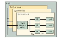
• Power density: To decrease size, because supplying higher current requires additional VRs (Voltage Regulator). The processor’s operating voltage is no longer scaling with transistor density, so the VR-supplied current is increasing. Today, each system board needs 10 to 100 or more VRs to supply 100A to 1,000A or more (e.g., up to 20,000A for a high-end server card). Each rack in a data center or network system has many system boards (Fig. 25-2).
25-2. Many Voltage Regulators (POLs) per System.
• Granularity: To support the massive parallelism of many small energy-efficient elements (e.g., many heterogeneous processor cores, micro-server cards, small-cell base stations, etc.). Benefits include more integration and specialization, reduced thermal loads, and better dynamic resource allocation, thereby providing high efficiency at low to medium loads. Many ICT systems will increasingly spend a large percentage of their time operating in low-power standby modes.
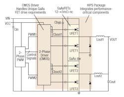
25-3. HIPS Module has two independent outputs or a two-phase input.
Moore’s Law scaling does not help the incumbent VR technologies, because they use many discrete components, such as controllers, MOSFETs, inductors, and capacitors. Due to MOSFETs’ high switching-power losses, today’s 12V, 10–30A VRs operate at a low (1.0MHz or less) switching frequency. This requires bulky inductors and capacitors, and they consume a large percentage of board space (~40%). They also suffer from a slow response time. MOSFETs are an aging 35-year-old technology and are hitting a performance asymptote. Moore’s Law scaling does not help MOSFETs, either, because they must withstand high voltage on the drain (e.g., 18–20V for 12V input). There are a finite number of well-known techniques for improving MOSFET performance, most of which have already been exercised.
More-than-Moore Scaling
More-than-Moore scaling requires heterogeneous Integration, the integration of separately manufactured components into a higher level assembly that in the aggregate provides enhanced functionality and improved operating characteristics. An example is the Heterogeneously Integrated Power Stage (HIPS) shown in Fig. 25-3. Its cross-section is in Fig. 25-4.
25-4. Cross-section of the HIPS module.
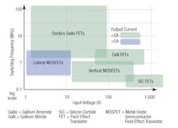
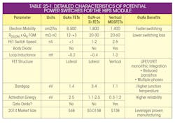
One of the important design decisions for the HIPS was selection of the optimum technology for the regulator’s power switch. This determination was aided by a comparison of the characteristics of GaAs, GaN, SiC, and silicon MOSFETs power switches, as shown in Fig. 25-5. This figure shows that GaAs FETs offer benefits over the other switches for voltage regulators operating with up to a 100V DC supply. Table 25-1 compiles the characteristics of GaAs, GaN, silicon MOSFET power switches.
25-5. Comparison of the switching characteristics of GaAs, GaN, SiC, and Silicon MOSFETs
The HIPS module uses the optimum technology for each function:
• Gallium arsenide (GaAs) for the field-effect transistors (FETs).
• CMOS for drivers, protection, and control, handling the GaAs FETs’ unique requirements.
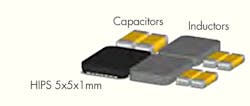
• 3D packaging using embedded die-in-substrate technology to integrate in a 5mm x 5mm x 1mm QFN package the GaAs die, CMOS driver die, and passive components required to minimize parasitics for the high switching frequency (Fig. 25-6).
An HIPS module is an evolutionary leap over the Driver-MOSFET (DrMOS) integrated power stage module. It replaces the MOSFET dies with a GaAs die, reducing packaging parasitics and integrating performance-critical components in a very small package. GaAs FETs have much lower switching-power loss than MOSFETs due to their superior intrinsic material properties: 5x higher electron mobility (8,500 versus 1,400 cm2/Vs), 5x lower on-resistance x gate charge (FOM), and no body diode (which eliminates reverse recovery loss). GaAs FETs also are more reliable, because they have no gate oxide, higher activation energy, higher bandgap, and the primary failure mechanism (sinking gates) is self-limiting.
The HIPS module can increase the voltage regulator switching frequency by 10x or more. Its switching frequency range of 2 to 5MHz reduces the size of the output capacitors and inductors while reducing the transient response time. An HIPS can readily be used in industry-standard synchronous buck converters with complementary components (PWM controllers and inductors) from third-party suppliers. No new architectures, materials, or components are required. A typical use for the HIPS is in point-of-load (POL) converters.
25-6. HIPS package contains passive and active components.
HIPS also increases the power density and granularity (providing more than one output) for board-mounted voltage regulators. The HIPS uniquely enables Package-Integrated Voltage Regulators (PIVRs) that integrate many fast, small VRs in the processor package as close as possible to the processor die without increasing its cost or heat dissipation.
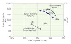
HIPS modules enable many fast, small VRs that can reduce the energy consumption of ICT systems by 30% or more through fine-grain power management of multi-core processors, energy proportionality and reduced cooling requirements. Fig. 25-7 compares the characteristics of a typical power MOSFET output stage with the first and second versions of the HIPS.
25-7. Comparison of the performance of a typical MOSFET output stage and the HIPS, Rev1 and Rev2. The Figure of Merit for Rev2 HIPS is 6mΩ-nC vs. 30mΩ-nC for a typical MOSFET output stage. These results are for a 12Vin and 1.2Vout power stage.
Samples of the HIPS were available in 2016 with full production scheduled for 2017.
Since VR-supplied current scales roughly with processor performance and price, we can check the processor market to estimate the HIPS market size. The market for processors, application-specific standard products (ASSPs), and FPGAs in data centers and network systems, the initial target markets for HIPS, is forecast to grow to $21.9 billion in 2018:
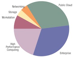
25-8. $10.3 Billion Market for Processors Used in Data Centers in 2018
(Source: The Linley Group)
• $10.3 billion for server processors, most of which are used in data centers (Fig. 25-8). Captive processors, such as IBM’s Power and Oracle’s SPARC, are excluded.
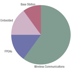
25-9. $11.6 Billion Market for Processors, ASSPs, and FPGAs Used in Voice and Data Networks in 2018 (Source: The Linley Group)
• $11.6 billion for processors, ASSPs, and FPGAs used in voice and data networks (Fig. 25-9). Communications semiconductors include components for Ethernet, broadband infrastructure, customer premise equipment, home/access networking, network processors (NPUs), transport (Sonet/SDH, OTN), PCI Express, RapidIO, and network search engines.
Assuming it’s approximately 5% of the processor content, the HIPS content for these systems is approximately $1.1 billion. HIPS modules also improve energy efficiency and, hence, the performance of ultrathin, fanless all-in-one desktop PCs, notebooks, tablets, and smartphones within a very challenging thermal envelope—a small, thin case that must remain cool enough to touch.
The GaAs industry today makes products for RF and microwave communications. In 2013, the industry produced 29.3 million square inches of GaAs, which is equivalent to 100,000 GaAs 150mm wafers per month. GaAs industry revenue exceeded $6 billion revenue in 2014. Hence, the GaAs industry has ample well-proven, high-volume manufacturing capacity for producing HIPS modules.
This concludes the Power Management series.

