How Does EMI Affect Various Electronic Systems? (Part 2)
This article is part of the TechXchange: Delving into EMI, EMC and Noise.
Members can download this article in PDF format.
What you'll learn:
- Defining EMI, including NIST's definition.
- How EMI affects a PCB's electronic systems.
- Minimizing EMI with SSFM.
In Part 1, we discussed electromagnetic interference (EMI) in spacecraft electric propulsion systems (EPS), communications equipment, radar, navigation systems, IFF systems, and wireless-power-transfer designs. Part 2 again addresses how EMI is defined and looks at its effects on PCBs and other digital systems, plus presents one method to reduce EMI.
EMI is essentially a disturbance caused by an electromagnetic field that prevents the proper performance in an electrical/electronic system. EMI can emanate from both natural and man-made sources, for example, the Sun’s or the Earth’s magnetic fields.
Most of the EMI that creates problems for precision research applications comes from stray magnetic or electrical fields that are generated by electrical machinery or electrical equipment. In the case of a data path, these kinds of EMI effects can cause problems ranging from an increase in error rate to a total loss of data.
The National Institute of Standards and Technology (NIST) defines EMI as “an electromagnetic disturbance that interrupts, obstructs, or otherwise degrades or limits the effective performance of electronics/electrical equipment.”
EMI will lead to poor operation, malfunctioning, and can even stop circuitry from working at all. System circuit designers need to design their architectures to prevent EMI disturbances that can negatively affect their electronics performance.
Man-made or even natural EMI sources can be minimized or even blocked via electrical shields. The choice of using higher-quality electronic components could help as well. Finally, error-correction methods4 may reduce EMI effects.
Let’s look at other examples as to how EMI can be prevented or at least minimized in electrical/electronic systems.
EMI in PCB-Based Electronic Systems
EMI will affect the performance of RF, clock, and digital systems on a printed circuit board (PCB).1 Voltage and current induction can happen in any region of a PCB, depending on the orientation and routing of the incident electromagnetic wave.
EMI Effects on the RF System
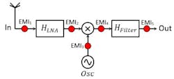
Voltage and/or current induction will occur in any region of the PCB depending on the routing and orientation of the incident electromagnetic wave. Figure 1 illustrates the output spectrum of the oscillator (Osc), with HLNA and HFilter as the transfer functions of the low-noise amplifier (LNA) and filter, respectively.
Shown is the total induced effect of EMI on an RF receiver PCB system. The orientation and routing of the incident electromagnetic wave leads to the voltage/current induction in any region of that PCB.
EMI Effects on Digital Systems
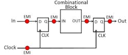
Just as in the section above, EMI also can be induced into each area of a sequential digital system (Fig. 2).1 Therefore, the voltage/current induction can happen to any region of the PCB depending on the orientation and routing of the incident EMI wave.
EMI Effects on an Information System2
The following study examines the possible impact of EMI on an information system composed of radar systems, communication stations, and an information processing center.
The performance of the information system, and particularly the digital communication system, must be evaluated. Possible EMI sources will mostly derive from neighboring radar systems. A thorough analysis will help optimize the design of an information system under this electromagnetic (EM) environment.
One thing to keep in mind is that digital microwave circuitry should be located more than 10 km from radar sources to prevent any EMI disturbance. This distance, though, will likely lead to higher system costs and additional system design requirements.
Let’s take a case of four sets of C-band radar stations (RS) that are quite close to the communication station (CS)—far less than 10 km. This will facilitate the transfer of the radar signal. Now, the electromagnetic-compatibility (EMC) design also will be more difficult and greatly affect the performance of the communication system networks.
Now, the communication network for the information system will need to exchange data and transmit between the radar and the control center. The major parameter for evaluating the performance of the communication system will be the bit error rate (BER).
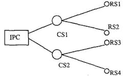
The information system under study is composed of four RS, two CS with four distinct means of communication links, and one information processing center (IPC). In this example, the RS communication is of most importance; the rest of the systems will be standby communication. Thus, only microwave communication will be relevant and studied in this example. Figure 3 shows a simplified topology of this information system.
Reducing EMI with Spread-Spectrum Frequency Modulation
Switching regulators are frequently deployed to power portable battery-operated designs in the form of dc-dc converters. These dc-dc switching regulator devices are quite efficient and will extend battery runtimes for power portable devices. Unfortunately, a drawback of these efficient dc-dc converters is the fast current switching that can lead to a significant EMI source, which will quite possibly disturb the operation of other surrounding electronic devices.
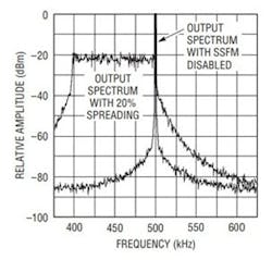
Enter spread-spectrum frequency modulation (SSFM), in which the EMI energy gets randomly spread amongst multiple frequencies instead of being concentrated at just one frequency. To do this, the clock must be able to generate an SSFM output to synchronize the switching regulator.
Spread-Spectrum Clocking
In the SSFM method, the clock output is constantly moving, unlike a steady clock output. Such a steady clock can be easily affected by locking onto nearby devices and even conformity test equipment. Consequently, these neighboring devices will accumulate emitted signal energy at the fixed clock frequency or even that clock’s harmonic signals.
We can compare spectra in Figure 4, which is a spectrum analyzer image of a square-wave clock signal. If SSFM isn’t used, most of the energy in the signal output is shown in Figure 2 at the programmed 500 kHz. When SSFM is turned on, the output frequency of the clock randomly shifts between 400 and 500 kHz. Figure 4 depicts a frequency change of 100 kHz, which is a 20% spreading.
Therefore, when SSFM is applied to a switching converter, the energy of the EMI at any high frequency will have an amplitude of 1/10 of a single, fixed clock frequency. The result of the lower amplitude frequency components reveals a marked reduction in EMI.
Summary
EMI is a disruption that can negatively affect an electrical circuit due to either electromagnetic induction or externally emitted electromagnetic radiation. EMI is defined as an interference, from one electrical or electronic system to another, generated via electromagnetic fields. This article presented more examples of how to prevent or minimize EMI disturbances in electronic systems.
Read more articles in the TechXchange: Delving into EMI, EMC and Noise.
References
1. “The Analysis of EMI Effects on the Performance of Electronic Systems Implemented on a PCB,” Advanced VLSI Lab, School of ECE, College of Eng., University of Tehran, Tehran, Iran, and the IEEE.
2. “The effects of EMI on the performance of Information Systems,” Lizhou Bai, Jianjian Song Institute of High Performance Computing Republic of Singapore.
3 “Easy-to-Use Spread Spectrum Clock Generator Reduces EMI and More”, Tim Regan, Doug La Porte.
4 “Resilience of Error Correction Codes Against Harsh Electromagnetic Disturbances: Fault Elimination for Triplication-Based Error Correction Codes,” IEEE Transactions on Electromagnetic Compatibility, Vol. 62, No. 5, October 2020.
About the Author

Steve Taranovich
Freelance Technical Writer, Phoenix Information Communication LLC
Steve is a contributing editor to Electronic Design.
Author of the non-fiction “Guardians of the Right Stuff,” a true story of the Apollo program as told by NASA and Grumman Corp. engineers, an astronaut, and technicians.
Experienced Editor-In-Chief of EETimes/Planet Analog and Senior Technical Editor at EDN running the Analog and Power Management Design Centers from 2012 to 2019.
A demonstrated history in electronic circuit design and applications for 40 years, and nine years of technical writing and editing in industry. Skilled in Analog Electronics, Space-related Electronics, Audio, RF & Communications, Power Management, Electrical Engineering, and Integrated Circuits (IC).
1972 to 1988 worked as a circuit design engineer in audio (8 years) and microwave (8 years). Then was Corporate Account Manager/applications engineer for Burr-Brown from 1988 to 2000 when TI purchased Burr-Brown. Worked for TI from 2000 to 2011.
Strong media and communication professional with a BEEE from NYU Engineering in 1972 and an MSEE from Polytechnic University in 1989. Senior Lifetime member of IEEE. Former IEEE Long Island, NY Director of Educational Activities. Eta Kappa Nu EE honor society member since 1970.
Voice Your Opinion!
To join the conversation, and become an exclusive member of Electronic Design, create an account today!

Leaders relevant to this article:
