This file type includes high resolution graphics and schematics.
As applications cross traditional vertical market boundaries and market segments are re-shuffled, IC companies are developing platforms for cell phones and tablets, using a single IC to target multiple mobile applications. The approach requires standard intellectual property (IP) interfaces for success in several product categories.
For example, a single application processor used in traditional mobile applications such as smart phones and tablets and mobile-influenced markets such as automotive infotainment systems, medical personal assistant devices, and sports equipment command and control units must be able to communicate effectively with the surrounding hardware.
The Samsung Exynos processor, for example, is used in a variety of Samsung products: small and large display smart phones, point-and-shoot cameras, and tablets. In these products, the main differences between the system-on-chip (SoC) used are the number of processor cores and the operating frequency.
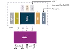
To effectively address multiple applications, the ICs must incorporate high-performance chip-to-chip interfaces that will support emerging mobile standards such as USB SuperSpeed Inter-Chip (SSIC) and Mobile PCI Express (M-PCIe), which utilize the MIPI M-PHY (Fig. 1).
Mobile Interfaces: Low Power, High Performance
Applications servicing mobile electronics and mobile-influenced markets continue to enhance the user experience, increase productivity, and enable new use models. The ICs used in these applications require high-performance core operation and high-speed interfaces with small area and low power consumption.
Common to all mobile and mobile-influenced applications is the requirement for low power in operation and in idle modes. Most mobile devices are idle for long periods, so efficiently putting the device in idle mode for long idle periods or in between operations can increase battery life and end-user satisfaction.
Related Articles
• Test Tools Debug And Validate MIPI M-PHY
• MIPI And PCI Express Join Forces
• Physical Layer Test Challenges And Solutions For MIPI Interfaces
Complex SoCs used in mobile applications incorporate features like high-resolution image capture and display, videos, and LTE data streaming, all of which need higher throughput and capabilities. High-performance interfaces enable the SoC to effectively connect to image sensor, display, and storage and wireless communication devices.
The table shows the power savings of a power-optimized physical layer (PHY) (M-PHY used for USB 3.0 SSIC implementation) compared to other PHY implementations. This illustrates the increased bandwidth and lower-power capabilities of the M-PHY in USB 3.0 SSIC applications.
As the mobile market demands very high-resolution, high-quality image capture and display, the interfaces must evolve to keep up. For example, existing MIPI CSI-2 image sensors, capable of driving 4 to 6 Gbits/s, fall short of the 10 Gbits/s or more required by the coming generation of applications offering multi-megapixel images, greater color depth, and better refresh rates.
Increased Need For Standard Chip-To-Chip Interfaces
As mobile electronics evolve, the SoCs need to support supplemental capabilities such as wireless connectivity, image sensor interface, and storage interface. These additional features require the SoCs to implement standard, high-performance, low-power chip-to-chip interfaces. General-purpose chip-to-chip interfaces provide flexibility to mobile electronics manufacturers when integrating their products.
For example, one mobile electronic device can incorporate LTE modem capability while a different mobile device, using the same SoC and interfaces, can connect to a WiGig IC to enable wireless connectivity. Using custom non-standard chip-to-chip interfaces is, in most cases, not an ideal strategy because it locks the solution to a specific vendor and does not provide the options and use of standards-based solutions.
SoCs are likely to implement general-purpose high-performance chip-to-chip interfaces such as the USB SSIC or M-PCIe interfaces. USB SSIC is based on the USB 3.0 protocol, which is typically used in consumer and mobile applications, while the M-PCIe interface targets laptops and PC peripherals. The USB SSIC v1.01 specification, defined by the USB Implementers Forum, is available now for implementation. M-PCIe specification is in review by the PCI-SIG member body and is expected to roll out in the second quarter of 2013.
Using the widespread, but different, USB and PCI Express ecosystems enables the reuse of software drivers in the SoC. Coupled with a low-power PHY implementation, relying on these ecosystems gives these mature interfaces a power-efficient implementation that can be adopted across multiple applications.
This file type includes high resolution graphics and schematics.
Ubiquitous USB SSIC And M-PCIe With MIPI M-PHY
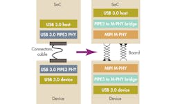
USB SSIC (Fig. 2) and M-PCIe interfaces utilize the MIPI M-PHY specification to provide a variety of low-power modes and reduce electromagnetic interference (EMI). The USB SSIC and M-PCIe specifications allow designers to use existing USB and PCI Express software drivers while connecting with the MIPI M-PHY and utilizing its low-power capabilities. This is particularly useful in mobile designs that already have a library of USB drivers.
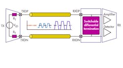
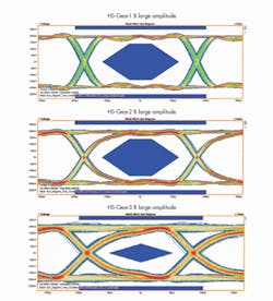
The MIPI M-PHY used in conjunction with these two protocols allows designers to implement multiple high-speed (HS) gears, from 1.25 to 5.8 Gbits/s, as well as low-speed pulse-width modulator (PWM) modes used for control. The M-PHY allows designers to implement two HS-Gear rates (A and B) for reduced EMI in the system. The M-PHY also enables large or small voltage amplitudes for low-power transmission as well as switchable termination (Fig. 3).
Mobile applications’ transmissions are typically “bursty,” and the M-PHY can address this challenge by enabling selectable high-speed and low-speed bursts. This burst-speed flexibility, along with a variety of low-power modes, provides the capability to select the exact burst speed required to deliver the data traffic with the lowest power consumption. Furthermore, the availability of multiple power modes allows the designer to utilize the most effective power mode that minimizes power consumption based on the application recovery time to operation.
For example, utilizing the M-PHY hibernate mode provides the lowest M-PHY power consumption with HS-burst recovery time in microseconds. On the other hand, utilizing the stall power mode allows a much faster recovery time to HS-burst operation but with less power savings. These options provide flexibility for the SoC to utilize the best practices to match the data traffic profile.
Figure 4 shows an abstracted way to consider burst speeds and low-power mode tradeoffs. The ultimate goal in reducing total system power is to burst the data as quickly as possible to reduce the power-per-bit metric and switch to the best available power mode for the lowest power consumption that matches the latency required to switch back to burst.
Using the MIPI M-PHY for the PHY, instead of the USB 3.0 or PCI Express PHY, enables significant power reduction in operation and idle modes. Coupling the maturity of the USB 3.0 and PCI Express ecosystems with the MIPI M-PHY creates mobile-friendly standards, making it easy for designers to adopt the standards and reduce power consumption in mobile devices.
MIPI M-PHY v3.0 For High Performance
After the MIPI M-PHY v3.0 specification was announced at Mobile World Congress 2013, Synopsys was the first IP vendor to demonstrate silicon-proven DesignWare MIPI M-PHYv3.0 IP operating in HS-Gear3 Rate B, which was shown at the March 2013 MIPI Alliance face-to-face meeting in Bangkok.
The availability of a compliant, silicon-proven M-PHY at the time of the specification release enables designers to reduce the risk of adopting the M-PHY for their storage and camera applications, as well as chip-to-chip interfaces including USB SSIC and M-PCIe and other UniPro-based controllers.
Conclusion
The MIPI M-PHY v3.0 specification allows designers to implement several protocols to match their increasing high-performance and low-power requirements in mobile devices. Readily available MIPI M-PHY IP supporting HS-Gear3 can enable designers to reduce their market and design risk while coupling the M-PHY with the mature and established USB SSIC and M-PCIe protocols.
This file type includes high resolution graphics and schematics.


