How to Wirelessly Power and Access a 1-Wire Network (Part 2)
To read Part 1 of this two-part article, click here.
1-Wire devices power-up parasitically by charging an internal reservoir from the 1-Wire communication line. VPUP, the pull-up voltage on the 1-Wire network, depends on VOUT and RPUP. The maximum current that can be supplied to the 1-Wire network also depends on these two parameters.
When powering a 1-Wire network from a high-impedance source like the MAX66242 voltage regulator at VOUT, enough time should pass until the devices attached to the 1-Wire network are charged and ready to communicate before sending 1-Wire function commands. A 1-Wire device is charged and ready to communicate when the initial capacitance CIO at its I/O pin is charged.
Most 1-Wire devices specify typical and maximum CIO values that exist on their 1-Wire I/O port. The maximum CIO exists when VPUP is first applied to the 1-Wire network. After the 1-Wire network is fully charged, only the typical CIO affects 1-Wire communication. Therefore, the CIO-MAX should be charged to the minimum pull-up voltage VMIN-PUP required by the 1-Wire device. Equation 1 defines the minimum pull-up voltage VMIN-PUP across the total maximum capacitance CTOTAL-MAX of the 1-Wire network:
where:
CTOTAL-MAX = ΣNi=0 (CMAX-IO, i + CLAYOUT)
RS+PUP = RS + RPUP
VMIN-PUP = minimum pull-up voltage required on the 1-Wire network
VS = open-circuit voltage at VOUT.
The capacitance CLAYOUT represents the capacitance introduced to the 1-Wire network because of junctions on the 1-Wire node (Fig. 1).
1. The 1-Wire network is modeled as a series of I/O capacitances CIO and parasitic layout capacitance CLAYOUT due to junctions on the 1-Wire node.
VMIN-PUP is the largest minimum-pull-up voltage that exists in the 1-Wire network. For example, if device number one has a minimum pull-up voltage of 2.8 V and the minimum for device number is 3.0 V, then VMIN-PUP should equal to 3.0 V for the 1-Wire network.
Equation 2 determines the time tCHARGE necessary to charge the total maximum capacitance CTOTAL-MAX to the minimum pull-up voltage VMIN-PUP of a 1-Wire network:
Parasitic Capacitance During 1-Wire Communication
The total typical capacitance CTOTAL-TYP on the 1-Wire network after powering up is defined as the sum of all typical capacitances CTYP-IO plus the parasitic capacitance of the layout CLAYOUT.
This is represented in schematic form in Figure 7 (see below) by replacing CMAX-IO,N with CTYP-IO,N where:
The typical capacitance CTYP-IO refers to the parasitic capacitance at the I/O that originates from each of the device’s internal 1-Wire receivers/transmitters. The typical capacitance CTYP-IO, the pull-up voltage VPUP, and the pull-up resistance RPUP are responsible for the following four fundamental timing parameters used in every 1-Wire communication sequence:
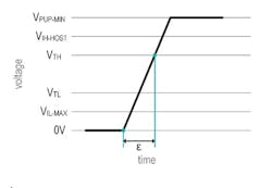
- ε = Time taken to pull up from 0 V to the 1-Wire network’s threshold-high voltage VTH.
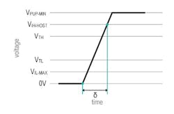
- δ = Time taken to pull up from 0 V to the 1-Wire host input-high voltage VIH-HOST.
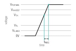
- tREC= Time taken to pull up from VTH to VPUP. tREC defines the maximum time available for the 1-Wire network to recharge during communication.
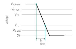
- tf= Time taken to pull down from VPUP to the 1-Wire network’s threshold-low voltage VTL.
Time constants ε, δ, tREC, and tf help specify a maximum total typical capacitance CTOTAL-TYP that can allow proper 1-Wire communication for a given RPUP and VPUP. If CTOTAL-TYP is exceeded, then timing constraints aren’t met, rendering 1-Wire communication improbable. Refer to the datasheet for the respective 1-Wire device to find the value of the four time constants.
Pull-up Fundamental Timing Parameters ε, δ, and tREC
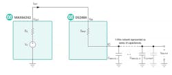
2. Time ε to charge the total typical capacitance CTYP-TOTAL from 0 V to VTH.
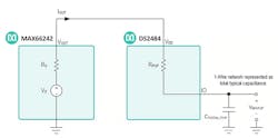
Figure 2 illustrates time ε needed to charge up the 1-Wire total typical capacitance CTOTAL-TYP from 0 V to VTH. Figure 3 presents this concept in schematic form.
3. Here, the 1-Wire network is modeled as an equivalent total typical capacitance CTOTAL-TYP that includes the parasitic layout capacitance CLAYOUT.
Equation 3 defines ε = Time required to charge CTOTAL-TYP from 0 V to VTH via RS+PUP:
Figure 4 illustrates time δ needed to charge up the 1-Wire total typical capacitance CTOTAL-TYP from 0 V to VIH-HOST.
4. Time δ to charge total typical capacitance CTYP-TOTAL from 0 V to VIH-HOST.
Equation 4 defines ε = Time required to charge CTOTAL-TYP from 0V to VTH via RS+PUP:
Figure 5 illustrates the shortest time tREC needs to recharge the 1-Wire total typical capacitance CTOTAL-TYP from VTH to VPUP-MIN.
5. Shortest time (tREC) that’s possible to charge total typical capacitance CTYP-TOTAL from VTH to VPUP-MIN.
The following three-step procedure shows how to calculate tREC.
1. Calculate the time required to charge from 0 V to VTH—this is equivalent to ε in Equation 3.
2. Calculate the time required to charge from 0 V to VPUP-MIN:
t’ = -RS+PUPCTOTAL-TYPln(1 – VPUP-MIN/VS)
3. Use the quotient rule to find tREC = t’ – ε:
Pull-Down Timing Parameter tf
Unlike ε, δ, and tREC, time tf doesn’t depend on RS and RPUP. This is because time tf defines the time required for the 1-Wire host or device to pull down the 1-Wire network. Therefore, the pull-down resistance RPDOWN of the 1-Wire host or device defines the time tf necessary to discharge CTOTAL-TYP from VPUP to VTL as illustrated in Figure 6.
6. Time tf to discharge total typical capacitance CTYP-TOTAL from VPUP-MIN to VTL.
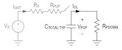
The pull-down resistance RPDOWN for the 1-Wire host and device is derived from the maximum output low voltage VOL and the corresponding output low current IOL given in the electrical characteristics table of the respective datasheet. Figure 7 illustrates the pull-down resistance RPDOWN and the pull-down current IOL.
7. This simplified RC circuit models the pull-down resistance RPDOWN from either the 1-Wire host or device.IOL is the pull-down current.
For example, the DS2484 I2C-to-1-Wire bridge has a maximum VOL of 0.4 V at 4 mA. This means that the maximum pull-down resistance of RPDOWN is 100 Ω.
Equation 6 defines the discharge time tf:
If the four fundamental parameters ε, δ, tREC, and tf are met for all devices on the network, then 1-Wire communication and power delivery are possible. By knowing the total allowable capacitance to meet all edge timings specified by the 1-Wire protocol, the maximum number of devices and bus length achievable in the NFC-powered system can be determined.
Compatible 1-Wire Devices
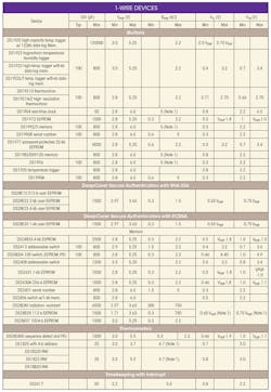
The table lists 1-Wire devices with their respective input/output capacitance CIO, pull-up voltage VPUP, pull-up resistance RPUP, voltage threshold-low VTL, and voltage threshold-high VTH specifications. VTL is the voltage below which, during a falling-edge on the 1-Wire network, a logic low is detected. VTH is the voltage above which, during a rising-edge on the 1-Wire network, a logic high is detected. Both VTL and VTH are a function of VPUP and 1-Wire recovery times.
Modeling an NFC transponder connected to a 1-Wire network as an RC circuit allows us to verify whether harvested power delivery and communication are feasible. A smartphone or any device equipped with an NFC transceiver under ISO15693 and FIPS180-4 can authenticate; identify; access memory from; conduct data acquisition on; and control a 1-Wire network. An NFC system can wirelessly power a 1-Wire network and allow secure asset and information management for a node of closed mobile systems and Internet of Things (IoT) devices.


