Smart Ideal Diodes Protect Car Battery Front-Ends
Members can download this article in PDF format.
What you’ll learn:
- Different reverse-polarity solutions and their effectiveness at providing car battery front-end protection.
- How a smart diode controller can provide optimal reverse-battery protection.
If the battery terminals in a car are reverse-connected during a jump start, vehicle maintenance, or repair, the components in the electronics control unit (ECU) may be damaged if they can’t handle this fault condition. On top of that, during normal operation, the car battery voltage isn’t constant—the input voltage (VIN) can even be negative under several transient tests regulated by the EMC standards, such as ISO 7637 and ISO 16750. These fluctuations mean that front-end protection is necessary.
Schottky diodes and P-channel MOSFETs (PFETs) are widely used in automotive power-system designs for reverse-battery protection and automotive electrical transient protection. However, these conventional solutions have significant power dissipation, which reduces thermal efficiency and makes it more difficult for designers to meet the system’s cost and space requirements.
This article presents a review of reverse-polarity solutions, using MPS’s MPQ5850-AEC1—a smart diode controller that can be used for automotive front-end protection—as an example. The article also explores the advantages of using a controller versus traditional front-end protection solutions.
Schottky Diodes for Front-End Protection
The Schottky diode is the simplest reverse-polarity protection schematic (Fig. 1). During normal operation, the diode (D1) conducts in the forward direction. When a reverse voltage is applied, D1 stops conducting.
Due to the diode’s constant and significant forward voltage drop, as the normal operating current increases, the power consumed on the diode also increases proportionally, which results in bad thermal performance. Thus, Schottky-diode solutions are typically only used for low-current conditions.
As time passes and better strategies are developed, it will become more difficult to meet system requirements with the Schottky diode due to its large reverse leakage and outdated architecture.
P-Channel MOSFETs for Front-End Protection
A PFET is commonly used for reverse-polarity protection in industrial and automotive applications because it results in a small voltage drop for low power loss. Figure 2 shows the schematic when implementing a PFET.
During normal operation, the current first flows through the PFET’s body diode, and the PFET’s source (S) voltage is close to the battery voltage (VBATT). At this juncture, the gate (G) voltage is 0 V—this is negative relative to the PFET’s source end, which is also the circuit’s output.
In such a scenario, the PFET (Q1) can conduct, and then the current flows from the drain (D) to the source (S). The solution’s Zener diode (D1) is able to protect the gate-to-source voltage (VGS) from exceeding the rated voltage.
When the system is under reverse-polarity conditions, D1 conducts forward, and VGS is only about 0.7 V. Then Q1 turns off to protect the system from damage caused by the reverse-polarity voltage.
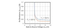
A PFET is self-biased by simply pulling its gate pin low, which means that the PFET has poor cold-crank performance (low VBATT operation). During severe cold cranks (where VBATT falls below 4 V), the PFET’s series resistance increases drastically (Fig. 3). This leads to a higher voltage drop across the PFET. During a cold crank, a higher gate-to-source threshold (VTH) can sometimes lead to a system reset if the PFET turns off.
However, using a PFET can pose certain challenges. PFET solutions need a protection circuit, which is composed of the Zener diode (D1) and current-limit resistor (R1) to avoid VGS exceeding its breakdown voltage (BV). Both D1 and R1 have a leakage current, which increases the system’s quiescent current (IQ). In addition, when adding an AC input voltage, the PFET is fully on, causing current backflow. This forces the electrolytic capacitor to repeatedly charge and discharge, ultimately leading to overheating.
Smart Ideal-Diode Controllers for Front-End Protection
The traditional reverse-polarity protection solutions described above struggle to meet many requirements for new systems, such as low cost, small space, high efficiency, and versatility. To meet these requirements, smart ideal-diode controllers that drive external N-channel MOSFETs (NFETs) have been developed.
The NFET must be placed on the high side; the smart diode controller IC also takes power from the high side. The internal supply voltage must exceed the battery voltage (VBATT) to drive the NFET. There are two methods to generate this supply voltage: charge pump and boost (Fig. 4).
Charge Pump
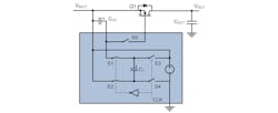
Figure 5 shows the working principles for the charge-pump method using four switches (S1, S2, S3, and S4). CT is a low-value capacitor with fast charging and discharging speed, while the charge pump capacitor (CCP) is a high-value capacitor with a large load capacity. When the pulse-width-modulation (PWM) signal of the clock is high, S3 and S4 conduct, and the internal source charges the CT. When the PWM signal is low, S3 and S4 open, S1 and S2 conduct, and CCP is charged by CT.
Therefore, through frequent switching between S1 and S2 (as well as S3 and S4), the charge on CT can be continuously transmitted to CCP. In addition, the CCP’s negative terminal is connected to the battery voltage (VBATT); therefore, the NFET can be driven by a voltage exceeding VBATT.
The charge pump has a low efficiency and weak driving current capability, which is usually only a 10- to 30-mA pull-up. When VBATT fluctuates rapidly (e.g., during an input superimposed high-frequency AC signal from ISO 16750-2 in Figure 6), it’s easy to generate abnormal phenomena, such as gate-drive pulse loss and gate-drive pulse constantly on.
If the gate-drive pulse is lost, the NFET remains off and the current is conducted by its body diode, resulting in a large amount of thermal loss. When the gate-drive pulse is constantly on, the NFET remains on and the output electrolytic capacitor (COUT) repeatedly charges and discharges, which can lead to overheating.
In addition, although the charge pump doesn’t have an inductor, the charge-pump circuit is a capacitive switching power supply that requires a very high operating frequency (fSW) due to its low efficiency. Usually, the integrated capacitance for CT is small (within the picofarad range) and the external capacitance for CCP is large (within the microfarad range). Therefore, the charge pump’s fSW often exceeds 10 MHz, which can lead to electromagnetic-interference (EMI) issues and a higher IQ.
In summary, the charge-pump solution has a lower overall bill-of-materials (BOM) requirement, but it’s only recommended for low-current applications as it lacks sufficient capacity for high-power applications.
Boost Converter
Figure 7 shows the working principles for a boost-converter solution. When S1 is conducting, the inductor is charged by VBATT, increasing the inductor current. Once the inductor current (IL) reaches the fixed peak current threshold, S1 is open. IL continues to flow through the diode (D1) and charges a capacitor (C1). When the voltage on C1 exceeds VBATT, the NFET’s gate is driven high.
When using a boost converter to drive an external NFET, the boost converter’s efficiency is relatively high. This converter can provide a greater driving current capacity (exceeding 100 mA) and faster input interference response. Therefore, a smart diode controller solution with an integrated boost converter is recommended for high-power applications. It can also achieve an excellent VIN rectification effect.
In addition, the boost converter uses fixed peak current-mode control, meaning the lighter the load, the lower the fSW. Since the NFET consumes only a small current, it results in a solution with extremely low fSW and almost no EMI issues.
A New Smart Ideal-Diode Solution
In response to the front-end’s demand for high current, fast response, and small footprint, MPS developed the MPQ5850-AEC1, which can be used for automotive front-end protection (Fig. 8).
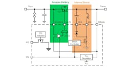
The MPQ5850-AEC1 is a smart ideal-diode controller that can drive an external NFET to replace a Schottky diode or a PFET for reverse input protection. The device integrates an internal boost to provide a boost voltage that turns on the external NFET, even at a low-input VBATT. Figure 9 shows the device’s functional block diagram.
The MPQ5850-AEC1 can regulate the source-to-drain voltage (VSD) to 20 mV by modulating the gate of the external NFET. The device’s 20-mV ultra-low dropout minimizes power loss and makes it possible to easily detect small negative currents.
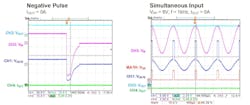
The 4-μA shutdown current and 30-μA IQ also make the device well-suited for battery-powered applications. The MPQ5850-AEC1 features a strong gate-drive ability (170-mA pull-up and 430-mA pull-down) for ultra-fast transient response. Moreover, it meets stringent ISO 16750 and ISO 7637 requirements such as Class 4 negative pulse and 100-kHz input superimposed high-frequency AC signals. Figure 10 shows a few test waveforms.
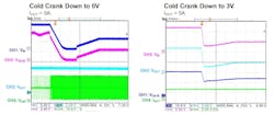
The MPQ5850-AEC1’s internal circuitry is powered by the drain voltage (VDRAIN) instead of VBATT. If VDRAIN exceeds its undervoltage lockout (UVLO) threshold, then the MPQ5850-AEC1 operates normally, even if VBATT drops to 0 V during a severe cold-crank condition.
If VDRAIN drops below the UVLO threshold, the device pulls down the GATE pin to the SOURCE pin (which is also the NFET’s source) until the voltage on the reservoir capacitor discharges below its UVLO threshold. This enables the device to minimize forward-voltage drops during temporary low-voltage transients, such as cold-crank conditions. Figure 11 shows the cold-crank test waveforms.
The MPQ5850-AEC1 also integrates an open-drain power-good (PG) signal pin to indicate certain statuses, such as when the boost capacitor is out of regulation, an overcurrent (OC) condition is active for longer than 17 μs, or the device is disabled. In the meantime, the internal boost uses the low-frequency, fixed peak current-mode controller, giving the MPQ5850-AEC1 excellent EMI performance (Fig. 12).
Comparing the Methods for Front-End Protection
For front-end protection, Schottky diodes can be used in low-current applications that are low cost and have a simple circuit. However, as the current increases, the power and thermal loss of the solution also become more severe. For higher currents, MOSFET circuits can be used instead, but a PFET or an NFET should be selected based on the specific application conditions. A PFET can’t be employed at low voltages, nor can it provide input rectification.
For the two methods using an NFET, the charge-pump drive solution has a lower overall BOM requirement, which can reduce costs. However, its electromagnetic-compatibility (EMC) performance is poor and more suitable for low-current applications, such as high-power charging modules for automotive USB power-supply devices.
A boost-converter solution, such as the MPQ5850-AEC1, can provide the required driving capabilities and EMC performance. The converter is recommended for high-current and high-performance environments, such as automotive domain controllers and audio systems.
The table summarizes the different solutions described in this article.
Conclusion
Four possible solutions can be used to provide front-end protection for car batteries, particularly for reverse polarity. Depending on an application’s needs, it may be advantageous to select any of these options, such as a Schottky diode, P-channel MOSFET, or a smart controller with N-channel MOSFET.
Using a smart controller such as the MPQ5850-AEC1 enables a complete solution while improving efficiency, minimizing EMI, and operating under harsh conditions (e.g., a cold-crank condition and input superimposed high-frequency AC conditions). On that front, MPS has a portfolio of automotive-grade smart controllers that can help meet design requirements.


