Bringing the Power of SiC to Data Centers Driving AI
Power is becoming the latest bottleneck to threaten progress in artificial intelligence (AI). To help tackle the looming power crunch, onsemi developed a new series of silicon trench power MOSFETs and silicon-carbide (SiC) MOSFETs.
Simon Keeton, president of power solutions at onsemi, said the combination of its Si and SiC MOSFETs can reduce the power losses plaguing data-center power supplies by as much as 1%, giving them higher efficiency and better thermal performance in a smaller area. By swapping the power FETs into data centers globally, he said it would be possible to save up to 10 terawatt-hours (TWh) of electricity per year.
Key to the solution is SiC. While it’s a relatively new material in power semiconductors, SiC is replacing silicon as the gold standard in high-voltage power switches. It’s more expensive but plays a pivotal role in EV traction inverters in between the battery pack and the motor: SiC power MOSFETs lose less power overall and can switch at faster rates, which helps save space and reduce system costs.
SiC is also bound to play a part in reducing the staggering amount of electricity that modern data centers are burning through to train and run computationally heavy AI. These vast clusters of servers consumed 2% of all global electricity—or around 460 TWh—in 2022. But technology giants and startups are hungry for even more power to stay relevant in the AI race, with the International Energy Agency (IEA) estimating at least 650 TWh by 2025.
On the high end, more than 1,000 TWh of electricity use is not out of the question, said the IEA.
Next-Gen AI Silicon Drives Up Demand for Power
Traditional CPUs, which each require around 300 W, aren’t the culprits in this case. The AC-DC power supplies used for high-voltage power distribution in data centers feed up to 10 of these chips, for a total of 3,000 W. The latest AI accelerators, e.g., NVIDIA’s Hopper GPU, are even more power-hungry, requiring up to 700 W each today, with its Blackwell GPUs rated to consume 1,000 W or more by 2025. By the end of the decade, a single data-center GPU that consumes 2 kW or more is a distinct possibility.
Such AI chips are driving up the power demands of data centers by 3X or more. The power consumed by just one rack of servers is rising to 90 kW and even as high as 120 kW, up from current levels of 15 to 30 kW.
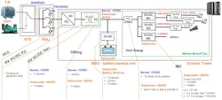
When electricity enters a data center from the grid, it’s converted several times before being used by the CPUs, GPUs, and/or AI chips at the heart of the server. The power-supply unit (PSU) is one of the first parts that the electricity runs into—it converts the mains AC used for high-voltage power distribution to regulated DC power at a lesser voltage that works for the server and the circuit board inside of it (see figure).
For years, the standard DC voltage to supply power to the server and over the PCB was 12 V. The power supply translated the AC mains from the grid centrally and bussed it to servers, where it was translated to a form that was usable for the processor’s cores. However, as power increased, the losses stemming from this approach started getting out of hand. As a result, tech leaders are upgrading to 48 V to reduce the current required by a factor of four, since Ohm’s Law states power is equal to current times voltage (P = I × V).
The other form of Ohm’s Law, which states that power equals resistance times current squared (P = R × I2), means that upping the voltage to 48 V reduces the losses caused by resistance on the power rails by 16X.
As the voltages used by the processor cores inside CPUs, GPUs, and other modern chips have decreased to less than a volt, you need several different voltage rails that can run at relatively high power. The solution is to add another DC-DC converter stage—called the intermediate bus converter (IBC)—which turns the 48 V from the power supply to a 12-V local bus voltage that can then be more efficiently converted to “core” by the voltage regulator modules (VRM) that bridge the “last inch” of the power-delivery network (PDN).
Some degree of power is wasted every time that power is converted from one form to another, resulting in heat that must be carefully managed. In the case of the “hyperscale” data centers, the Amazons, Googles, and Microsofts of the world require 120 kW of rack power to run the CPUs, GPUs, and other silicon at the heart of AI servers. As it happens, about 12% of the electricity ends up wasted before entering the GPU, creating 15 kW of heat that must be dissipated, in many cases with water or other forms of liquid cooling.
“Power losses are a double-edged sword: the losses are wasted energy with a cost,” noted Aditya Jain, senior director of product management at onsemi, “and they generate heat which requires space and further cost to manage.”
He added that to wring as many inefficiencies out of data-center power supplies as possible, companies are investing in everything from more advanced power topologies to new approaches such as synchronous rectification.
The MOSFET: The Key to Solving the AI Power Pinch
But what matters most is the MOSFET at the heart of the switch-mode power supplies (SMPS) in data centers. To keep pushing the limits of system efficiency and power density, these power devices must be as efficient as possible.
While silicon has been at forefront of power electronics for decades, onsemi is bringing SiC into data centers with its latest 650-V MOSFETs, which offer superior switching performance and lower device capacitances. One of the most valuable properties of SiC is that it can handle higher breakdown voltages than Si, ranging from hundreds to thousands of volts, giving it the edge for data-center power distribution.
These chips also have a higher mobility of electrons in the channel, which is the space under the gate that sends current from the source to the drain of the switch. Thus, they turn on and turn off significantly faster than IGBTs or other silicon power FETs, reining in power losses that can add up during the switching process.
Not only is SiC superior when it comes to power handling, but it also has higher thermal conductivity, enabling more efficient cooling. These FETs can operate safely at higher operating temperatures, too.
According to onsemi, the EliteSiC MOSFETs reduce gate charge by 50% and limit the total energy stored in output capacitance (EOSS) and output charge (QOSS) by 44%, for minimal conduction losses. By eliminating the tail current during turn-off, they also lessen switching losses compared to superjunction (SJ) MOSFETs. Furthermore, heat is managed more efficiently than silicon, which helps further limit switching losses. These upgrades give you the ability to increase operating frequency and, thus, use smaller passives and magnetics.
The T10 PowerTrench series of silicon MOSFETs is engineered to handle high currents—crucial for DC-DC power-conversion stages—and offers higher power density and superior heat dissipation in a very compact footprint. The improvements are largely due to the underlying “shield gate trench” construction of the power FET, giving it minimal gate charge and reducing on-resistance (RDS(on)) to less than 1 mΩ.
The soft recovery body diode limits the reverse-recovery charge (QRR), minimizing ringing and noise while reducing the risk of overshoots. That helps maximize performance, reliability, and robustness of the device.
Other companies are rising to the challenge of delivering power to AI silicon as well. Infineon rolled out a reference design for a PSU that not only contains Si and SiC power switches, but also power FETs based on gallium nitride (GaN)—the other rising star in power semiconductor material.
Read more articles in the TechXchange: Silicon Carbide (SiC). Also check out more of our coverage of PCIM 2024.
About the Author
James Morra
Senior Editor
James Morra is the senior editor for Electronic Design, covering the semiconductor industry and new technology trends, with a focus on power electronics and power management. He also reports on the business behind electrical engineering, including the electronics supply chain. He joined Electronic Design in 2015 and is based in Chicago, Illinois.


