Silicon Capacitors: The Future of Mobile SoC Power Delivery?
Members can download this article in PDF format.
What you’ll learn:
- Mobile SoCs are progressing to finer process nodes to pack more computing power in a smaller space while slashing power consumption.
- These high-performance chips operate with lower supply voltages while simultaneously increasing the magnitude of di/dt (load steps), highlighting the need for strict control on power-supply noise.
- Why the best way to refine power integrity at the “last inch” is to place low-impedance components as close as possible to the power-supply pins and why silicon capacitors such as ECAPs fit the bill.
In smartphones, IoT devices, and similar high-performance applications, power delivery is becoming the difference maker. Supplying power smoothly and efficiently over the “last inch” of the power distribution network (PDN)—immediately before it hits the application processor—is arguably the biggest challenge facing systems engineers today.
The challenge stems from the high-frequency power demands of these very high-performance chips. As one of the most basic and fundamental components in electronics, capacitors are the go-to component for smoothing out the rapid delivery of power to these mobile SoCs, and they’re used in large quantities across a variety of such designs. While traditional multilayer ceramic capacitors (MLCCs) have fulfilled the requirements thus far, stricter constraints on power density are challenging the existing model.1
As system engineers look to deliver on their promises for higher performance in smaller form factors, provisioning the most efficient power decoupling solution is critical.
In this article, we examine the decoupling requirements of a typical mobile-phone design and the electrical parameters that are critical in the choice of components, as well as make the case for integrating decoupling capacitors to SoC substrate. We then further discuss how E-CAPs can effectively improve the performance of SoCs compared to traditional MLCCs.1
Smartphone Development Trends
As technologies continue to improve in 5G, foldable displays, and AI, the smartphone industry is expected to continue advancing rapidly in the coming years.
Several analysis firms predict the following evolutionary trends for smartphones in the next few years:
- More powerful computing resources: Clock frequencies have increased by 30%, and ML benchmark scores have increased by 3.2X in the past three years.
- Continuous integration of functional blocks: Baseband, ISP, game acceleration, and neural-network units have been integrated to mobile phones. Support for functions like AI on the edge along with advances in biometrics, AR, and VR are expected to be added soon.
- Higher bandwidth memories for higher computing resources will follow the same trend as in AI computing.
- Longer battery runtime is needed, driving new materials and power-efficient SoCs.
- Foldable phones are likely to continue to develop, offering users a larger display that can be folded for portability.
Challenges in Power Design
Smartphone SoCs need to integrate more transistors while reducing power consumption to meet the stated requirements. To achieve that goal, manufacturers need to use more advanced semiconductor processes, and larger chips, which bring about three important challenges to power design.
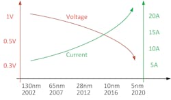
The first challenge is the stringent noise requirement for advanced processes. Operating voltages for computer chips are shrinking. With an increasing number of transistors, the peak current demand is becoming larger. Figure 1 shows the trend of the change in operating voltage and current over the past 20 years.
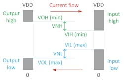
Figure 2 and Equation 1 illustrate the allowable power noise for the processor core voltage. A large part of the performance depends on the quality and speed of digital communication between the different parts of the system. Hence, the noise immunity is driven by signaling logic levels.
Higher noise tolerance (VNH and VNL) leads to better noise immunity. However, lower operating voltages drive the high and low signal windows to be smaller, resulting in the chips being more sensitive to power-supply noise.5
Where:
- VNH is the high signal noise tolerance.
- VOH is the minimum output high voltage.
- VIH is the minimum input high voltage.
- VNL is the low signal noise tolerance.
- VOL is the maximum output low voltage.
- VIL is the maximum input low voltage.
The second challenge is to handle fast dynamic loads. Modern processors run highly dynamic workloads, such as running large AI algorithms on demand. In general, for portable applications, execution of tasks is completed as fast as possible at peak performance, followed by long periods of lower performance states, driven by the need to increase battery life. For such applications, the peak current swings become significant, with instantaneous peak processor currents of up to 30 A in 10 ns becoming the norm. This results in extremely challenging (di/dt) current transients.1
The latest SoC requires power-supply ripple to be at the level of 15 mV or less, driven by the lower supply voltages and noise margins. Power-supply specifications typically include accuracy, transient, and output-voltage ripple targets. In addition, multiple application notes have been published that also highlight the need for power integrity (PI) analysis.2
The third challenge comes from the size. To support stronger computing performance, manufacturers are also increasing the chip size. However, this leads to increased power consumption of the SoC and shrinking space for the power supply.
All of the above means that the power supply should provide more power, less noise, and support larger dynamic loads in a smaller area. This sets very strict requirements for power-supply quality.
Overcoming the Power Challenges
Power engineers have come up with many ways to address the power challenges, including the following methods:
- Adaptive voltage scaling (AVS), multi power domain, and power gating technology: These approaches supply each necessary individual processor domain on a SoC with just enough voltage so that it can deliver the required performance while minimizing power consumption per task.3
- Increasing the number voltage-regulator phases: In a multiphase regulator, the effective ripple frequency is multiplied by the number of phases, with each phase supplying a reduced current ripple to the output capacitors shifted in time. These combined properties make it possible to reduce the output ripple without increasing the output capacitance.2
- Increasing voltage-regulator switching frequency: This is the holy grail of switching regulators. One benefit is to significantly increase the power density. It allows the power supply to be placed much closer to the load. Another benefit is that increasing the frequency widens the voltage-converter bandwidth, resulting in smaller voltage droop, and orders of magnitude faster recovery during fast load transient. For example, Empower’s IVR technology offers the industry’s highest switching frequency, which enables 4X size reduction and 10X faster transients.
- Close decoupling of the processor: The benefits of placing decoupling capacitors close to the load are critical. It significantly shortens the decoupling path, greatly reduces the parasitic parameters, and thus means that the AC impedance seen by the load will be greatly reduced.
The first three methods are widely known to substantially reduce the power noise and average power usage. This article focuses on how to design a good decoupling capacitor and solutions that help improve the PDN performance.
The Risk with Parasitic Parameters
Real-world electronic components aren’t ideal, and they’re saddled with parasitic parameters along with the component’s primary electrical parameter.
Parasitic parameters can cause dynamic voltage droop during fast dynamic transient and increase power noise. To ensure the IC is working properly, engineers need to make sure the operating voltage along with the noise spikes are always within window of the maximum and minimum supply-voltage specifications. Often the noise is due to fast transients that cause voltage droops, needing a higher nominal supply voltage. Referring to Equation 2, this will result in an increase of power consumption.4
Where:
- PLoss is power loss of the chip.
- PStatic is static steady loss. Relates to the input voltage and the leakage current.
- PSwitch is switching loss. Relates to load capacitance, the square of the input voltage, the operation frequency, and the activity factor k, which is proportional to the power-supply noise.
- PShort is short-circuit loss. Not only relates to the input voltage and short-circuit current, but also correlates to a factor caused by the rise and fall speed.
Considering these factors, adequate decoupling is needed to reduce supply voltage and power consumption. Equation 3 is the voltage drop during load transient4 based on the parameters of the decoupling capacitor. To minimize the dynamic voltage droop, ESL should be as small as possible, and Cd should be large to keep the ratio of ESL/Cd small. By optimizing the PDN, the dynamic voltage droop can be reduced, and hence the power loss. Thus, a good decoupling capacitor with the lowest parasitics in the right location is the key to optimize the PDN.
Where:
ESL is loop parasitic inductance.
ESR is loop parasitic resistance.
Cd is decoupling capacitance.
α = ESR/2 ∙ ESL is damping factor.
ω = 1/√ESL ∙ Cd is natural oscillation frequency.
Decoupling for Mobile SoC
Reference 1 discusses the importance of decoupling for high-performance processors. In short, the purpose of using decoupling capacitors is to ensure PDN AC impedance meets the requirements as shown in Figure 3.
To obtain the target impedance curve, it’s necessary to extract all of the trace parameters in the network and perform simulation with the PDN capacitors. This article doesn’t go into the details of the parameter extraction process, but it does directly use the parameters from a design case to compare the effects of different capacitors.
There are many locations to place the decoupling capacitors (Fig. 3, again). As described by Equation 3, a decoupling capacitor with a low ESL-to-capacitance ratio should be placed as close to the load as possible. For a typical SoC, it’s optimal to embed the decoupling capacitors into the SoC substrate, as this is the closest to the load, followed by placing them on the bottom of the substrate.
With technology continually maturing, advanced packaging capabilities have enabled mobile SoC manufacturers (Fig. 4) to integrate decoupling capacitors on the package’s landing (bottom) side. These capacitors provide the optimal power integrity during fast and large transients, due to the shortest path (and hence lowest parasitics) to the supply pins of the SoCs. Such integration helps in managing larger transient currents by reducing the PDN impedance and simultaneously simplifying the PCB level design.
Due to the need for portability while offering rich functionalities, every component in a mobile phone needs to be extremely compact. Therefore, unlike the PCB-mounted capacitors or general CPU bottom-mounted capacitors, there are strict size and height requirements for capacitors placed on the substrate bottom of a mobile phone's SoC.
As shown in Figure 5, due to the height restriction of the BGA balls, it’s preferred that the total height of capacitors on the substrate bottom not exceed 100 µm after soldering. Besides, the board area should not exceed 1 mm2 to avoid removing too many BGA balls.
From Equation 3, we know that good decoupling capacitors require a small ratio of ESL to capacitance. However, as pointed out in Reference 1, the inherent ESL of MLCCs is quite large. The effective capacitance is also much lower than preferred in ultra-thin situations. These characteristics conflict with the demand to reduce the power droop and noise.
Emergence of E-CAP
E-CAP is an example of a silicon-based capacitor that’s ideally suited to meet the requirements outlined earlier. E-CAP is based on a high-precision, deep-trench, silicon-wafer process. This process significantly reduces the basic unit size of capacitors. In turn, there’s an order-of-magnitude reduction in the length of internal electrode plates and, consequently, a similar order-of-magnitude reduction in ESL. By connecting hundreds or thousands of silicon capacitor units in parallel to form a single high-capacity E-CAP, the ESL is further minimized.
In addition, silicon capacitors exhibit no variation due to voltage bias, as well as negligible temperature and aging degradation. Silicon capacitors also offer dramatically improved product reliability, driven by the use of a limited number of materials, a proven silicon fabrication process, and chip-scale packages.
Figure 6 compares the parameters of commonly used decoupling MLCCs for mobile SoC packaging with the Empower E-CAP for high-performance computing. It shows that E-CAP can provide several times higher effective capacitance in unit area and 100X lower ESL of MLCCs.
E-CAP Improves Mobile SoC Power Integrity
The previous sections discussed the development trends of mobile phones, which further highlights the importance of decoupling for mobile-phone SoCs. This section discusses how performance improves by integrating E-CAP in the substrate bottom compared to MLCCs based on actual mobile phone design.
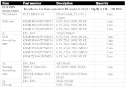
Figure 7 shows a typical PDN from the voltage-regulator module (VRM) to the load point. For processors based on TSMC’s 7-nm process, the typical PDN requirements and parameters for the APU and CPU are shown in Figure 8.
Based on these parameters, we use SIMetrix-SIMPLIS to perform impedance and transient simulations to compare the differences between E-CAP and MLCC as the package decoupling caps. They’re mounted in the same location on the bottom side of the substrate.
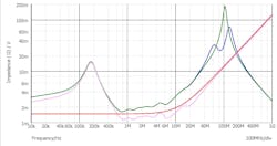
Figure 9 reveals the impedance simulation results with the same PCB components, but only the substrate bottom capacitors are changed. It’s clear that the PCB level impedance (in pink) meets the SoC’s design target. By comparing the blue and green curves, the impedance near 100 MHz is reduced substantially by using E-CAP, and the maximum impedance with E-CAPs (74 mΩ) is only 40% of that with MLCCs (188 mΩ).
Figure 10 shows the transient response simulation of a 0 to 20 A in 10 ns on the left, and on the right side is the zoom in view of the transient spike. After using E-CAP, the transient droop decreased from 167 to 142 mV, a 15% reduction. As pointed out in Equation 2, power-supply noise may affect the processor’s power consumption. According to simulations from cellphone manufacturers, a 15% noise reduction may increase battery usage by 3% to 5%. This improvement was achieved by simply replacing a capacitor, and it requires minimal effort.
Overall, silicon capacitors such as E-CAPs significantly improve SoC power transient noise versus MLCCs. But this example replaces capacitors in only a single location. If all power-supply decoupling is similarly addressed, there’s potential for even larger gains in power integrity and a resulting improvement in mobile performance and battery life.
Read more articles in the TechXchanges: Charging Capacitors and Power Supply Design.
References
1. M. Krishna and L. Vassalli, "Addressing Power Decoupling in High-Performance, High-Frequency Applications Using E-CAP," IEEE Power Electronics Magazine, vol. 10, no. 3, pp. 29-35, Sept. 2023, doi: 10.1109/MPEL.2023.3301415.
2. Empower Semiconductor, AP-EP70xx-2 - Optimizing IVR Design for Low Noise Applications.
3. Frank Dehmelt, Application Report: “Adaptive (Dynamic) Voltage (Frequency) Scaling – Motivation and Implementations,” Texas Instruments
4. Raj Nair, Donald Bennett, Whitepaper: “Beyond IR Drop: Dynamic Voltage Droops and Total Power Integrity,” Anasim Corp.
5. D. Hodges, Analysis and Design of Digital Integrated Circuits, McGraw-Hill, Inc., July 2003.
6. Mark Alexander, Application Note: “Power Distribution System (PDS) Design: Using Bypass/Decoupling Capacitors” xapp623, Xilinx.
7. Erwan Petillon, Application Report: “Power Delivery Network Analysis,” Texas Instruments.
8. “Qualcomm Snapdragon 888 5G(SM8350) Specification,” HeadShotReviews, December 2020.
9. Hadlee Simons, “Snapdragon 8 Gen 2 vs Dimensity 9200: Which chip will reign supreme?” androidauthority.com, November 2022.


