Comparing Photodiodes: GaN PIN Avalanche vs. PIN
What you’ll learn:
- What is a PIN avalanche photodiode (APD)?
- What is a PIN photodiode?
- How to characterize avalanche breakdown in GaN.
Major differences exist between a PIN photodiode and an avalanche photodiode (APD), such as:
- Gain isn’t provided in a PIN photodiode; however, high gain and high speed via an internal gain mechanism is provided in an APD.
- An undoped intrinsic layer is strategically placed between two highly doped regions in a PIN diode, whereas a π layer is positioned between a p and n region in an APD.
- An amplifier is necessary to connect externally for a PIN diode, but no external amplifier is needed in an APD.
- A PIN diode has less response time, while an APD offers a very fast response time.
- PIN diodes have a small output current; APDs have higher output current.
- In a PIN diode, different noise currents are photon noise, shot noise, Johnson noise, and generation recombination noise. APDs have different noise currents such as shot noise, thermal noise, and avalanche noise.
- PIN diodes have shot current of Ishot = √2qIDB; APDs have shot current of Ishot = √2q (Iph + IB + ID)G2FB.
- PIN diodes have less sensitivity, while APDs possess higher sensitivity to detect very low light levels.
- PIN diodes need a low reverse bias; APDs require high reverse bias.
- PIN diodes have good temperature stability; APDs have poor stability.
Now let’s look at some technical details and applications for GaN-based APDs and PIN photodiodes.
What are PIN Photodiodes?
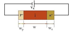
The PIN photodiode is a specialized semiconductor device that’s able to convert light energy into an electric current (Fig. 1).
The PIN diode is widely employed in such applications as optical communications and sensing to scientific research and medical imaging.
Characteristics of a PIN photodiode include:
Reverse bias operation
- Operates under reverse bias voltage (the N side is connected to the negative terminal and the P side is connected to the positive terminal).
- The reverse bias voltage will increase the width of the depletion region, which enhances the light absorption ability of the photodiode.
Fast response time
- The fast response time enables the PIN photodiode to respond to, and detect, light signals quickly.
- Such fast response time is critical for applications that need the modulation or detection of high-frequency light signals.
High sensitivity
- PIN diodes are quite sensitive to light. This allows them to detect weak light intensities or low-level light signals.
- The high sensitivity to light enables PIN diodes in applications suitable for demanding environments or those that need accurate detection when in low-light conditions.
Low noise
- Low-noise performance is critical in applications that need precise measurements and high signal-to-noise ratios.
- PIN diodes will exhibit low-noise characteristics that minimize distortion or interference of weak light signals during detection.
Wide spectral response
- Different semiconductor materials may be selected to optimize the photodiode response to specific wavelength ranges.
- PIN diodes will exhibit a broad spectral range, which enables them to detect light across a wide wavelength range.
- The specific spectral response range will depend on the material used in the photodiode.
What are GaN-based Avalanche Photodiodes (APDs)?
APDs have a similar structure to a PIN or PN photodiode,1 but they also have the following qualities:
- High speed and high gain via an internal gain mechanism.
- The ability to detect very low light levels with quite fast response times.
- They’re available from 100s of microns, and as high as 16 mm in active area diameter.
APDs are compact, robust, and lightweight when compared to a photomultiplier tube (PMT). They’re ideal for applications that need durability, a small envelope space, ability to survive in harsh environments, and are portable.
APD applications include LiDAR and time-of-flight rangefinders, optical communications, medical imaging, semiconductor fabrication equipment, molecular imaging, flame detection, and sensors for various chemicals and ozone.
Enabling Ultraviolet (UV) Light Detectors
At present, the dominant UV light detectors are based on PMTs, which have a high cost and low lifetime.1
Solid-state-based APDs look attractive for UV light detections because they can change the landscape of UV detection with more durability, lower cost, and exceeding the performance of a tube-based multiplier. APDs are highly sensitive photodetectors that can convert a light signal into an electrical signal, then amplify it by exploiting the carriers’ multiplication during impact ionization and avalanche.
Enabling a GaN APD with robust avalanche capability has two requirements:
- The presence of high-quality epitaxial layers, which is made possible when grown on free-standing GaN substrates.
- The use of optimized edge terminations that will eliminate both a dark leakage in the device and a localized peak electric field.
From many reports on the observation of avalanche, the homogeneous growth method based on free-standing GaN substrates, enabling a lower defect density of 103–106 cm−2, is essential for avalanche robustness. GaN APDs were also grown on bulk GaN, which fulfilled the first requirement of high-quality, low-defect-density (LDD) epitaxial films.
An edge termination that provides extra negative charges to terminate the electric field lines at the device boundary will reduce any localized peak electric field at any surface or corners, which is critical for the realization of an APD.
Characterizing Avalanche Breakdown in GaN
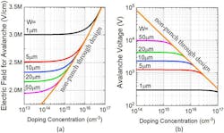
In Figure 2, the maximum electric field is presented as a function of doping, with the lightly doped region width (W) as a parameter. It’s clear in Fig. 2a that the maximum electric field for avalanche, in the thicker samples, will avalanche at a far lower electric field.11
For a given doping density of 2.4 × 1015 cm-3, by solving Equation 1, readers will find a fully depleted, drift region thickness in a non-punch-through (NPT) design to be close to 50 µm. This compares to an avalanche electric field of 2.5 MV/cm. When leaving the doping the same, the drift region thickness is reduced to achieve the punch-through (PT) design. Then for the 1-µm-thick drift region, a higher electric field value (approximately 3 MV/cm) would be needed to reach the avalanche condition.
It's critical that the correct value of α and β, as a function of the electric field be used to solve Equations 1 and 2, leading to the plots in Figure 2 in conjunction with Equations 3 and 4 below.
Where:
- W = depletion width
- EC = critical electric field
- Nd = donor density
- BV = breakdown voltage
- εS = permittivity of the semiconductor
- q = electronic charge
Equations 1 and 2 may be solved to determine an avalanche condition for any device structure that has arbitrary electric-field profiles. Devices that are limited by avalanche (e.g., power diodes and transistors) or depend on avalanche (e.g., APDS and impact ionization avalanche transit time, or IMPATT diodes) will have completely different electric-field profiles. Designers can classify them into two general categories:
- The NPT design has a triangular electrical field in the high-voltage region (Equations 3 and 4).
- The PT designs have trapezoidal fields to nearly rectangular (or nearly constant) electric fields.
Vertical power devices, such as DMOS devices, are designed so that the lightly doped (voltage-bearing) region width is chosen to be close to, but larger than the maximum depletion region width at reverse bias, an NPT design.
The Advent of APDs
APDs can offer UV light detection with better durability and lower cost, and they will surpass the performance of a tube-based multiplier. APDs are also highly sensitive photodetectors that can convert a light signal into an electrical signal. Furthermore, the APD amplifies that signal by taking advantage of the carriers’ multiplication capability during impact ionization and avalanche.
References
1. “On the Scope of GaN-Based Avalanche Photodiodes for Various Ultraviolet-Based Applications,” Dong Ji, School of Science and Engineering, The Chinese University of Hong Kong, Shenzhen, China; Department of Electrical Engineering, Stanford University, Stanford, CA, United States, Srabanti Chowdhury, Department of Electrical Engineering, Stanford University, Stanford, CA, United States, Frontiers in Materials, March 11, 2022, Volume 9, Article 846418.
2. “PIN Photodiode: It’s working Principle, Construction, VI Characteristics,” June 30, 2023 by rashikagupta1985.
3. “Low Leakage and High Gain GaN p-i-n Avalanche Photodiode With Shallow Bevel Mesa Edge Termination and Recessed Window,” Zhiyu Xu, Theeradetch Detchprohm, Shyh-Chiang Shen, Senior Member, IEEE, A. Nepomuk Otte, Member, IEEE, and Russell D. Dupuis, Life Fellow, IEEE; IEEE Transactions on Electron Devices, IEEE 2024.
4. “Avalanche Photodiodes—Design and Applications,” Oleks Goushcha, Ph.D., OSI Optoelectronics, March 2, 2021.
5. “Robust avalanche in GaN leading to record performance in avalanche photodiode,” Dong Ji, and Srabanti Chowdhury, Department of Electrical Engineering, Stanford University; Burcu Ercan, Department of Electrical and Computer Engineering University of California, Davis; Garret Benson, Department of Physics and Astronomy San Francisco State University, 2020.
6. “Single-Event Transients in a PIN Photodiode and a Single-Photon Avalanche Diode Integrated in 0.35µm CMOS,” Michael Hofbauer, Member, IEEE, Bernhard Steindl, Kerstin Schneider-Hornstein, 18th European Conference on Radiation and its Effects on Components and Systems (RADECS), Bernhard Goll, Member, IEEE, Kay-Obbe Voss, and Horst Zimmermann, Senior Member, IEEE, 2018.
7. “Avalanche Photodetectors, Marktech Optoelectronics.
8. “Al0.8Ga0.2As Avalanche Photodiodes for Single-Photon Detection,” Min Ren, Member, IEEE, Xiaoguang Zheng, Yaojia Chen, Xiao Jie Chen, Member, IEEE, Erik B. Johnson, Member, IEEE, James F. Christian, Member, IEEE, and Joe C. Campbell, Fellow, IEEE.
9. “Linear Mode Avalanche Photodiode With High Responsivity Integrated in High-Voltage CMOS,” Bernhard Steindl, Reinhard Enne, Stefan Schidl, and Horst Zimmermann, Member, IEEE; IEEE Electron Device Letters, Vol. 35, No. 9, September 2014.
10. “Crosstalk Effects of Avalanche CMOS Photodiodes,” Meng-Lin Hsia, Zhe Ming Liu, Chieh Ning Chan and Oscal T.-C. Chen, Dept. of Electrical Engineering, National Chung Cheng University, Chia-Yi, 621, Taiwan.
11. “On impact ionization and avalanche in gallium nitride,” Dong Ji, Srabanti Chowdhury, Stanford University, Applied Physics Letters, AIP Publishing, 2020.
About the Author

Steve Taranovich
Freelance Technical Writer, Phoenix Information Communication LLC
Steve is a contributing editor to Electronic Design.
Author of the non-fiction “Guardians of the Right Stuff,” a true story of the Apollo program as told by NASA and Grumman Corp. engineers, an astronaut, and technicians.
Experienced Editor-In-Chief of EETimes/Planet Analog and Senior Technical Editor at EDN running the Analog and Power Management Design Centers from 2012 to 2019.
A demonstrated history in electronic circuit design and applications for 40 years, and nine years of technical writing and editing in industry. Skilled in Analog Electronics, Space-related Electronics, Audio, RF & Communications, Power Management, Electrical Engineering, and Integrated Circuits (IC).
1972 to 1988 worked as a circuit design engineer in audio (8 years) and microwave (8 years). Then was Corporate Account Manager/applications engineer for Burr-Brown from 1988 to 2000 when TI purchased Burr-Brown. Worked for TI from 2000 to 2011.
Strong media and communication professional with a BEEE from NYU Engineering in 1972 and an MSEE from Polytechnic University in 1989. Senior Lifetime member of IEEE. Former IEEE Long Island, NY Director of Educational Activities. Eta Kappa Nu EE honor society member since 1970.


