How to Boost Speed and Efficiency for High-Transient Automotive Apps
What you'll learn:
- Using a multiphase buck-converter topology for high-current, low-voltage automotive applications.
- Implementation of coupled inductors in the multiphase buck topology.
- Test results of a voltage-regulator four-phase building block.
As advanced driver-assistance systems (ADAS) and other high-current applications proliferate in automotive applications, the computing power of the related GPUs and ASICs continues to rise significantly. This puts additional pressure on the performance of voltage regulators for such demanding loads, where the currents increase and transients become larger and faster.
Efficiency expectations continue to grow at the same time, while the load voltages decrease below 1 V for better thermal management and to enable advanced semiconductor processes with faster clocks. As low load voltage proportionally slows down the unloading transient and therefore causes a large increase in the bypassing capacitance, the voltage tolerance and transient specs are also tightening.
This calls for smaller and faster inductances in the multiphase voltage regulator to support such aggressive transients. The question is where patented Analog Devices coupled inductors can support the fastest current slew rates, while simultaneously minimizing the current ripple and supporting high efficiency in a small solution size.
Meeting High-Current App Needs with Multiphase Bucks
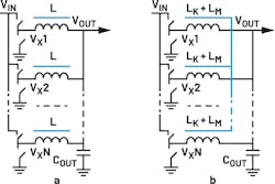
High-current, low-voltage applications frequently employ a multiphase buck-converter topology for the voltage step down. This multiphase buck can utilize traditional discrete inductors (DL) (Fig. 1a) or coupled inductors (CL) (Fig. 1b). In the case of CL, the windings are magnetically coupled, providing the advantage of current ripple cancellation.1-6
Automotive ADAS applications face a challenge in maintaining tight regulation for GPU or ASIC rails within the 0.4- to 1-V range, especially under fast transient conditions. A loading transient generally causes all phases to turn the switching nodes VX high to VIN. Thus, the inductor current in each phase ramps up with a slew rate (1), where VIN is input voltage, Vo is output voltage, and L is inductance value. An unloading transient typically causes all phases to turn low to GND and the inductor current ramps down (2).
Given the low output-voltage value VOUT < 1 V and assuming that the input voltage is typically 5 V or even higher, it’s easy to see from the comparison of Equations 1 and 2 that the unloading transient creates the main problem as there’s only a small voltage to ramp the current down.
The simple solution involves increasing the number of ceramic output capacitors in COUT. However, the size and cost of this approach can swiftly become impractical.
In the automotive industry, voltage regulators are often configured to switch at a relatively higher frequency (FS), typically exceeding 2 MHz. This is in contrast to regulators in cloud or industrial applications. The higher switching frequency is necessary in automotive settings due to specific electromagnetic-interference (EMI) requirements. While this choice helps to decrease inductance values in the regulator, further enhancements are still required.
The current ripple in each phase of the conventional buck with DL can be found as Equation 3, where the duty cycle is D = VOUT/VIN, VOUT is the output voltage, VIN is the input voltage, L is inductance value, and FS is the switching frequency.
Replacing the DL with CL, which has a leakage inductance LK and the mutual inductance LM, the current ripple in CL can be shown as Equation 4.6 The term defined as figure of merit (FOM) is expressed as Equation 5, where NPH is the number of coupled phases, ρ is a coupling coefficient (Equation 6), and j is a running index, which just defines an applicable interval of the duty cycle (Equation 7). The parameters of the CL are the leakage inductance LK and the mutual inductance LM.
The meaning of FOM in Equations 4 and 5 for the particular CL design can be interpreted as an additional multiplier in current ripple cancellation as compared to the conventional buck with discrete inductor L. The definition of FOM and its meaning were also generalized and extended11 to compare any systems with arbitrary current ripple and transient performances.
The proposal is to use a ratio of the normalized transient slew rate (desired high) to the normalized current ripple (desired low) (Equation 8). The transient slew rate and the current ripple are normalized by related numbers for some benchmark converters with discrete inductors (therefore, any system with DL will still lead to FOM = 1). The SRTR and ΔIL are transient current slew rate and current ripple in a steady state of the chosen design or technology, while SRTR_DL and ΔILDL are the same parameters but for the benchmark DL design.
Equation 8 can be simplified into Equation 9, using the fact that the current slew rate for the discrete inductor is the same in transient and steady state. This way, any actual reference to DL design is completely removed, while the benchmarking ideology is still there.
Notice that using the generalized FOM definition, Equation 9, for the CL will result in Equation 5. Thus, the new definition is backward compatible, but can also be used for technologies where both current ripple and transient slew rate are arbitrarily different from the DL equations (for example, TLVR9).
CL Design and Considerations
The application specifications are VIN = 5 V, VOUT = 0.8 V, FS = 2.1 MHz, and NPH = 8. As a starting point, DL = 32 nH is chosen to support the fast transient, while each inductor occupies 4.2 × 4.2 × 4.2 mm. Ideally, these would be substituted with an eight-phase coupled inductor, or CL. However, the low height requirement of h = 4 mm presents a challenge, as it would make such a lengthy component unmanufacturable due to being excessively thin and long, while also increasing sensitivity to board flex.
Therefore, the four-phase building block was chosen for CL. This also enables better flexibility with placement and layout. As the faster transient is targeted, and knowing that the CL will have smaller ripple than the starting DL value, the recently introduced Notch CL (NCL) structure was proposed to minimize the leakage value LK.7,8,10 The NCL0804 was designed with LK~17 nH and OCL = LM + LK = 100 nH, NPH = 4, phase pitch = 6.9 mm/phase, and a height h = 4.0 mm max (Fig. 2).
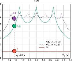
A good way to compare different designs is a FOM plot.10 Any DL design will have FOM = 1, as the tradeoff between the current slew rates in steady state and transient is 1:1. The NCL structure of the coupled inductor maximizes LM/LK ratio in a given size, so it generally results in the highest FOM.9 The FOM comparison is shown in Figure 3, where the developed NCL is ~4.4X better than DL around the targeted output voltage.
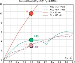
The corresponding current ripple comparison is shown in Figure 4 and the table. While the DL value can be chosen in a wide range for a different compromise between current ripple and transient slew rate, the advantage of developed NCL is always 4.4X. This correlates to 2.35X smaller current ripple than the ripple of DL = 32 nH, while NCL is 1.88X faster. Then 2.35 × 1.88~4.4, matching the predicted FOM = 4.4.
The current ripple can also be lowered substantially by using DL = 100 nH, which makes it 1.33X smaller current ripple than that in NCL. However, NCL is then 5.88X faster, resulting in the same 5.88/1.33~4.4X advantage of NCL over any DL (FOM = 4.4 for NCL).
When looking at a theoretical FOM for the same NCL in Figure 3, but considering if NPH = 8 is manufacturable, the performance advantage of NCL over DL would increase from 4.4X to 5.8X and make even more relative difference at a lower VOUT.
Looking ahead, it might be worth considering a different design for the NCL. One possibility is arranging the phases in two rows to maintain a low aspect ratio (length/height) of the ferrite core, making it conducive to manufacturing. In this scenario, the NCL could be positioned at the bottom of the PCB, directly above the ceramic bypass for the GPU, with power stages surrounding the NCL on the perimeter.
That approach, akin to a vertical power delivery (VPD) arrangement, could enhance the tradeoff between transient and ripple (effectively transient efficiency). However, it’s crucial to note that implementing such a change would be a significant departure from the existing design and layout. Whether this proposed approach is considered in the future will depend on customer preferences.
Experimental Results of the Voltage-Regulator Four-Phase Building Block
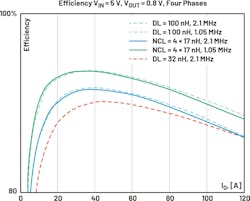
The 17 nH/phase NCL (Fig. 5b) offers ~1.9X faster current slew rate in transient and generally improves the phase margin in the feedback loop. Stepping down on ripple with DL = 100 nH (Fig. 5a) recovers the efficiency (Fig. 6), but such DL is significantly taller than the allowed h = 4-mm height, while also being ~5.9X slower than developed NCL. The latter would cause extreme implications for the amount of needed output capacitors. The results confirm the fundamental performance advantage of NCL as expected from the FOM estimates, against the different tradeoff options of the discrete inductor approach.
Substituting the DL = 32 H inductors with NCL0804-4 resulted in enhanced efficiency (Fig. 6). This improvement is mainly attributed to the significant reduction in current ripple (Fig. 4), leading to lower rms currents in windings, power stages, and traces. In addition, it contributes to lower AC losses, as depicted in Figure 6.
Conclusion: NCL Coupled Inductor Helps Optimize Performance
In summary, a new coupled inductor with the NCL structure was developed to optimize performance for an application with very low output voltage and aggressive load transient specifications. This CL was also built to fit the specified low profile for the automotive design. The NCL structure was chosen to minimize leakage, achieving a formal benefit of over 4X in transient/ripple performance compared to the conventional discrete inductor option.
To match the efficiency of the developed NCL, a discrete inductor (DL) with 1.6X the height (DL = 100 nH) would be needed. However, this alternative would fall 5.9X behind in transient speed, significantly impacting the size and cost of the output capacitance. The comparison in presented in the table highlights the advantages of the NCL0804-4 in terms of height, efficiency, current ripple, and transient speed.
References
1. Aaron M. Schultz and Charles R. Sullivan. “Voltage Converter with Coupled Inductive Windings, and Associated Methods.” U.S. Patent 6,362,986, March 2001.
2. Jieli Li. Coupled Inductor Design in DC-DC Converters. M.S. thesis, Dartmouth College, 2002.
3. Pit-Leong Wong, Peng Xu, P. Yang, and Fred C. Lee. “Performance Improvements of Interleaving VRMs with Coupling Inductors.” IEEE Transactions on Power Electronics, Vol. 16, No. 4, July 2001.
4. Yan Dong. Investigation of Multiphase Coupled-Inductor Buck Converters in Point-of-Load Applications. Ph.D. thesis, Virginia Polytechnic Institute and State University, July 2009.
5. Alexandr Ikriannikov and Di Yao. “Addressing Core Loss in Coupled Inductors.” Electronic Design News, December 2016.
6. Alexandr Ikriannikov. “Coupled Inductor Basics and Benefits.” Analog Devices, Inc., 2021.
7. Alexandr Ikriannikov and Di Yao. “Switching Power Converter Assemblies Including Coupled Inductors, and Associated Methods.” U.S. Patent 11869695B2, November 2020.
8. Alexandr Ikriannikov. “Evolution and Comparison of Magnetics for the Multiphase DC-DC Applications.” IEEE Applied Power Electronics Conference, March 2023.
9. Amin Fard, Satya Naidu, Horthense Tamdem, and Behzad Vafakhah. “Trans-inductors Versus Discrete Inductors in Multiphase Voltage Regulators: An Analytical and Experimental Comparative Study.” IEEE Applied Power Electronics Conference, March 2023.
10. Alexandr Ikriannikov and Di Yao. “Converters with Multiphase Magnetics: TLVR vs CL and the Novel Optimized Structure.” PCIM Europe, May 2023.
11. Alexandr Ikriannikov and Brad Xiao. “Generalized FOM for Multiphase Converters with Inductors.” 2023 IEEE Energy Conversion Congress and Exposition, October 2023.
About the Author
Jon Wallace
Senior Director, Analog Devices
Jon Wallace received his B.S. degree in computer and electrical engineering from Purdue University. Jon has been working in the automotive industry for 30 years. Prior to joining Analog Devices, Jon worked for 11 years as a software and hardware engineer at TRW Automotive Inc., developing hardware and software for safety electronics. In 2005, he joined Maxim (now part of ADI) as a product definer for automotive power and related products.
He has 25 issued U.S. patents in the fields of vehicle bus communications and software algorithms. The revenue for his defined products has exceeded $800M to date.
Issac Siavashani
Principal Engineer, Analog Devices
Issac Siavashani is a senior application engineer for the Automotive Business Team at Analog Devices. He received his MSEE degree in embedded system and electrical engineering from San Francisco State University.
In 2010, he joined Maxim (now part of ADI) and focused on multiphase buck management ICs for Intel (consumer) definition and development. In 2017, Issac joined the Maxim Integrated Automotive Business Team. He is currently working on high-current multiphase systems and radar PIMICs for low-noise applications.
Alexandr Ikriannikov
Fellow, Analog Devices
Alexandr Ikriannikov is a fellow for the Communications and Cloud Power Team at Analog Devices. He received his Ph.D. degree in electrical engineering from Caltech in 2000, where he studied power electronics from Dr. Slobodan Ćuk. His graduate school projects ranged from power factor correction for AC-DC applications from 15 to 400 V DC-DC for Mars rovers.
After graduate school, he joined Power Ten to redesign and optimize multi-kW AC-DC power supplies, and then in 2001 joined Volterra Semiconductor, concentrating on low-voltage, high-current applications and coupled inductors. Volterra was acquired by Maxim Integrated in 2013, which is now part of Analog Devices. Currently, Alexandr is a senior member of IEEE. He holds more than 70 issued U.S. patents, plus more pending, and has authored multiple publications in the field of power electronics.


