Can Advanced Packaging Break the Mold in Power Management?
From state-of-the-art materials and process technology to advanced circuit design and packaging, Texas Instruments has more than one way to maximize the power density of its products. But out of all these capabilities, advanced packaging is becoming more of a make-or-break technology in the pursuit of power density, said Jeff Morroni, TI’s director of power management R&D. And he’s right in the thick of things at Kilby Labs, TI’s research unit, which he joined after the company acquired National Semiconductor over a decade ago.
TI has rolled out a wide range of power modules in recent years that integrate capacitors, transformers, and inductors, placing them in the same package to boost power efficiency, dissipate heat, and reduce electromagnetic interference (EMI). But it aims to further close the distance between passives and power devices with its novel 3D magnetic packaging technology, known as MagPack. Instead of placing the magnetics next to the power device, TI said it uses a proprietary material to “mold” the inductors around the DC-DC converter in the module.
Placement of capacitors and transformers in a power supply can pose lots of difficulties for designers. But integrating the inductors in a way that enables the smooth, stable delivery of DC power tends to be the most challenging part of the power design due to strict thermal and space constraints. By placing the power inductor on top of the DC-DC converter, Morroni said MagPack can help alleviate many of these problems.
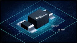
TI stated DC-DC converters based on its MagPack technology can make better use of height, width, and depth to increase power density at the system level. The company said these power devices are up to 50% smaller than previous generations, contributing to power densities of close to 1 A per square millimeter. The space savings have the potential to push them into data centers and other areas where power modules aren’t as prevalent at present.
For Morroni, passive integration and other types of advanced packaging are becoming a difference maker not only at TI, but also around the power industry. One possibility is the co-packaging of capacitors and inductors inside the chips they are feeding power to. Further out, he also sees the potential to integrate voltage regulators in the form of chiplets in the same package. This could be key to powering future generations of AI chips, which must be placed as close as possible to the core power supply to curtail losses and heat.
The following discussion has been edited and condensed for clarity.
Is there anything you wish you had known about the current situation in power electronics three years ago—or even 10 years ago? Is there anything happening today that you think caught you—or even the broader industry—off-guard?
I don’t know if I would say I was surprised by this, but it is interesting to see just how much more important power management has become to our customers over the last decade. At times, engineers have viewed power as a necessary evil. If I want to build a processor into my system, I inevitably need to power it somehow, but that’s just the details. What I’ve observed is increasingly how important power management is to the center of the system.
>>Check out the TechXchange and Library Series for similar articles and videos
Just think about the applications relevant today: electric vehicles, renewable-powered electric grids, and, within the last year or so, what has happened with AI. When you start thinking about all these different areas, you start to realize that power management is sort of at the heart of many of the biggest challenges that engineers are facing from generation to generation. If I think back 10 years ago, it just didn’t feel like that.
It’s interesting. I think AI is becoming a bigger topic not only because of the need to generate huge amounts of electricity, but once it enters the data center, you have to squeeze it all into the server, the board, and the package—and the closer you get to the processor, the more problems arise. Look at the latest AI accelerators. They are surrounded by a massive number of capacitors to manage all that power.
That’s right. Even if I think back a year ago, there were those in the industry predicting currents of 1,000 A to 1,500 A flowing into these AI processors a year from then, which would be about now. But what I have been noticing is that currents are already rising to 2,000 A or 3,000 A. So, even our predictions about how much power and how much current these chips are going to consume a year from today will probably be outpaced by reality.
Another thing we’re starting to see is the capacitors under these AI chips being replaced by power modules. That’s because the amount of current entering the chip is so high you need to put the power module even closer to the processor. The term for that is “vertical power.” And that’s sort of surprising in the sense that we’re seeing a rapid evolution of power electronics to meet the needs [of AI]. It’s much more a critical path than a necessary evil.
Is that the main power-related challenge in today’s data centers? These incredibly high currents?
I think it’s probably the fundamental one, but the implications trickle through the rest of the system. So, companies placing power modules under the processor to handle all the current is just one example.
To put it into context, when you have a thousand amps, you may have a very small amount of resistance between the output of the DC-DC converter and processor. But that resistance can still generate hundreds of watts of loss, and that’s just in the wire that connects the output of the voltage regulator to the processor. So, that drives the need to get the power module closer to the load.
Then you take it a step further, and companies are doing 48-V power distribution instead of 12-V. And then if you take it one step even further back into the grid, you want to do three-phase AC to the power-supply unit (PSU) because the amount of power that’s required just continues to scale. So, I think it all starts with the processor, but the implications go all the way to the grid.
So, how is packaging playing into the trend of power density? Where does it come into the picture?
Power density is one of TI’s guiding lights. But it’s difficult. To me, it’s like a balloon. When you squeeze one side, the other side pops out. You have power efficiency—the amount of power loss you experience—which is related to how much heat you generate. That prevents you from shrinking the power module because it will get too hot if you make it smaller without addressing those losses. So, that has always been the challenge.
So, while we’re a semiconductor company, what I think what we’re seeing moving forward is that the passives and magnetics—and specifically the inductor—are becoming a limiting factor in being able to drive power density higher. If you pull the power inductor inside a module, there is still the challenge of thermals, and the overall power density will be limited. So, how can I integrate these passives, particularly the magnetics, into the package?
Compared to some of the other areas in the world of power electronics—new developments in process technology will always matter [as will new materials for power semiconductors such as GaN]—packaging is becoming more and more important when it comes to enabling greater power density. That is also the case for applications such as server power, where power density isn’t just nice to have. It’s becoming a necessity at this point.
Take me through TI’s MagPack technology. What makes it different from other solutions around the industry or even within TI?
Coming out of Kilby Labs, this technology started as an R&D project close to a decade ago, so it has been a long time coming. What we started out trying to address is this elephant in the room with the power inductor being a major limitation on the power density.
There are power modules out there that are built more conventionally, and TI also has a portfolio of those. But what’s different about this is that we developed a 3D packaging molding process that enables very tight integration of the power inductor inside the package with virtually no overhead in the overall area compared to the chip. At its core, it was a materials development. So, we engineered a completely new magnetic material that enables us to integrate it as closely as we do while maintaining quality [and in a way] that is compatible with existing semiconductor processes.
So, do you normally place the inductor next to the power device inside the module? Is that the approach TI is trying to replace with MagPack?
There are a lot of different ways to do it traditionally. You can take the power inductor and place it next to the power converter in the module. But when you do that, the power density is not much better than just placing it next to the DC-DC converter on a PCB. I can’t discuss all the details of the MagPack technology. But we put the power converter through a molding process, and, as a by-product, we can build the power inductor at the same time. What that gives you is a device that looks like a chip but with the inductor inside of it.
Besides power density, are there any other benefits you’re seeing from integrating the inductor so closely with the power device?
So, the higher power density implies several other advantages. One of the bigger ones is the higher efficiency, so depending on what you compare it to, we’re seeing between 2% and 4% higher efficiency for modules based on the MagPack technology. That’s particularly important because if I’m going to build a smaller solution, almost by definition, I need to increase efficiency to get the heat out of the smaller footprint.
The other one is the thermal resistance of the package. If I’m generating a certain amount of heat, I can get more heat out of the package for a specific temperature rise with a more thermally capable package. And so, in this case, depending on what you compare it to, we are seeing something in the range of 20% better thermal resistance for these modules versus some of the more standard approaches.
The last one—and I’ll admit, we were not looking to do this when we started—is related to electromagnetic interference. So, the way we constructed the power module we ended up reducing the EMI, specifically the radiated emissions.
I think all these improvements will open new markets for power modules where you may have previously opted for a more conventional discrete solution because of limitations in power density, power efficiency, and EMI—and the ability to get the heat out.
In general, do you see advanced packaging playing a bigger role in the future of power electronics, you know, relative to all the other usual levers that you pull to improve power density?
Absolutely, I think so. But, as usual, I think it can get complicated depending on the specific application. There are different aspects of advanced packaging that are driving power density trends.
In power electronics, we’re not exactly on Moore’s Law. It’s more “More Than Moore” at this point. We’re not scaling the same way that the most advanced processors do. So, we need to solve the problem of power density in a different way than you would with transistor density, and advanced packaging is becoming the sort of critical element that can enable these solutions—or that can hold us back in terms of power density.
If we focus on the data center, I think that there are things that semiconductor companies can do to drive more heterogeneous integration, specifically with multichip modules (MCMs) that combine different capabilities and technologies.
Capacitor integration is a good example. The input capacitors for these power converters and how close they can be placed to the silicon is one of the more dominant mechanisms that decides how efficient you can be and how high frequency you can operate. So, we package the capacitors inside to hit the next level of efficiency. But when you start to do that, you realize that the closer you can place the capacitor to the power switches inside the silicon, the better performance you can get. Heterogeneous integration and 3D packaging—those all become tools in the toolbox.
The primary benefit of capacitor integration is to reduce the parasitic loop inductance on the input side of the DC-DC converter. This parasitic inductance can cause many nonidealities in power conversion, including lower efficiency, more EMI, and reduced device reliability. By integrating capacitors as close as possible to the power FETs, you reduce the impact of this parasitic inductance.
I wanted to clarify what you said about heterogeneous integration and 3D packaging. Will these technologies only be used to integrate passives more tightly with power converters? Or will we start seeing power devices co-packaged with the processors they are feeding power to? As in, you put a power chiplet and the passives in the same heterogeneous package as a CPU or a GPU?
We are seeing both. Integrating more passives into our package is definitely one technology roadmap. This is the primary vision for the MagPack technology.
In addition, we are also trending towards more chiplet style integration, on the same substrate or the same package as the CPU [or] GPU. This is often referred to as integrated voltage regulators or IVRs. Although this type of technology is not mainstream, as processor current goes higher and higher, IVRs will likely become a critical part of the power technology needs and roadmap.
Do you have any other thoughts on where this is all headed?
I kind of have a couple of answers to that. But I think one other category we haven’t touched on is that I think we’re going to see more co-development of solutions with semiconductor companies such as TI and our customers. As you integrate everything more closely, you have more degrees of freedom to co-optimize the processor, the substrate, the package, and then the power-management solution. That is a packaging challenge in the end, in addition to all the regular challenges with power converters. So, it’s an exciting opportunity for the power industry in general.
>>Check out the TechXchange and Library Series for similar articles and videos
About the Author
James Morra
Senior Editor
James Morra is the senior editor for Electronic Design, covering the semiconductor industry and new technology trends, with a focus on power electronics and power management. He also reports on the business behind electrical engineering, including the electronics supply chain. He joined Electronic Design in 2015 and is based in Chicago, Illinois.
Voice Your Opinion!
To join the conversation, and become an exclusive member of Electronic Design, create an account today!

Leaders relevant to this article:


