In Pursuit of Robust, Higher-Speed Power Designs with GaN

- How GaN provides superior power designs compared to silicon.
- Why LLC resonant topologies are best.
Traditional power transistors have long contributed to power losses (aka lower efficiency) in switching power-supply designs. Lossy power switching and conduction that occur in these power transistors fall into two categories:
- Switching losses: Power transistors are typically a main contributor to power losses within a switching power supply.
- Conduction losses: These losses are usually caused by a flow of current when the transistor is on, along with switching losses that typically occur in the transition between off and on states.
When gallium-nitride (GaN) transistors are turned on, they will look like a resistance that’s between the source and drain. This is typically referred to as the on-resistance (RDS(on)). Conduction losses are proportional to RDS(on).
>>Download the PDF of this article, and check out the TechXchange for similar articles and videos


Some GaN Applications
GaN usage in a low-voltage isolated DC-DC converter for aircraft provides excellent power density. To achieve a high power density, each stage of the power converter must be optimized to get full benefit of the topology that’s chosen.
For example, a MORE Electrical Aircraft (MEA) needs a solid power density coupled with a 270-V DC high-voltage DC (HVDC) bus along with a 28-V DC bus that has a low-voltage DC (LVDC) battery for safety (Fig. 1).
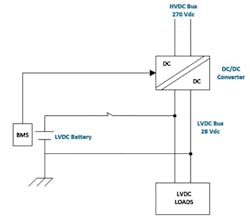
The high-voltage 270 V DC reduces the volume and mass for the aircraft electrical network.
Three topologies were selected:
- DAB (dual active bridge)
- LCC (resonant topology with series and parallel capacitors)
- LLC (resonant topology with series and parallel inductors)
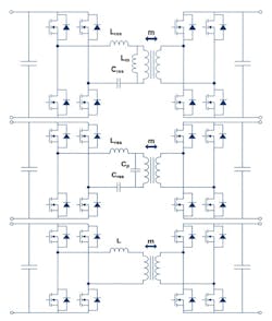
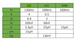
There will be a compromise between component values, resonant current, and voltage across the passive component, which leads to the 8-kW converter in Figure 2 being sized as a single converter.
The Winner is LLC
The best choice was the LLC, which is better suited to reach a high mass power density even though an added high-frequency (HF) capacitor was required (this capacitor element ensures that no saturation will occur in the transformer) (Fig. 3).
Because the output current is critical, the converter design is split into four modules, each with 2 kW in parallel. This was done because:
- Avoidance of paralleling GaN devices, since they will not be easily addressed for good current sharing.
- HF capacitors will have better availability, using 100 nF instead of 330 nF.
- Use a PCB design instead of a busbar output on the secondary side.
- MOSFET performance and lower losses that will enable the reduction of the heatsink.
GaN high electron mobility transistors (HEMTs) are used in the primary bridge, leading to low losses with high switching commutation. Custom passive transformer and capacitor components facilitate integration with good power density.
The power-density performance in this converter is 1.3 kW/kg. Extrapolation at the ambient temperature of 40°C, along with a powerful optimization of the converter, will lead to a power density of almost 2kW/kg. This is a successful objective for a power converter in an aircraft application (Fig. 4).
GaN for LiDAR
Light detection and ranging (LiDAR) has a plethora of applications, such as drones, automotive, robotics, retinal imagers, speed measurement devices, range finders, surveying equipment, and many more.4
LiDAR has a transmission system that sends out a brief high-current light pulse. This pulse bounces off objects and subsequently returns to a receiver. The time between the signal leaving the transmitter and returning is used to calculate the total distance that the pulse has traveled.
Transmitting signals faster will lead to higher-accuracy results because more data can then be interpreted by the receiver. Gate drivers are important here since they’re able to send multiple pulses at very high speeds, leading to high-frequency operation.
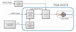
Low-side drivers tend are quite common for LiDAR applications. Texas Instruments has two recommended GaN gate drivers for LiDAR: the LMG1020 and LMG1025-Q1.
These two gate drivers enable high-frequency applications, nanosecond pulse widths, and a short propagation delay. They will drive a FET to produce an optical laser pulse of less than 1.5 ns at a power higher than 100 W.
Some of the key components of the LiDAR reference design in Figure 5 include a pulse-shortening buffer that creates nanosecond pulse widths, an LMG1020 GaN FET gate driver that drives a GaN FET to produce 60-A 1-ns laser optical pulses exceeding 100 W, and a laser diode.4 The driver pulses the GaN FET on and off so that the laser diode can send multiple pulses that will map objects and their distances.
GaN in a High-Speed Synchronous Buck DC-DC Power Converter
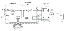
GaN HEMTs are featured in a multi-MHz power design tailored for high-speed DC-C converters.5 Texas Instruments’ LMG1210 is a half-bridge GaN driver that uses GaN power HEMTs. Applications include 5G telecom power, industrial power supplies, and telecom servers (Fig. 6).
The Benefits of GaN in Power Design
The power of GaN enables robust power designs, and GaN devices also help achieve smaller size with higher efficiency in such designs. The technology improves conduction losses and reduces switching losses.
Furthermore, GaN doesn’t have a body diode to lower losses obtained during dead-time. The current that would flow through the body diode of a silicon transistor will now flow through the RDS(on) with GaN. This substantially reduced the losses incurred during dead-time.
References
1. ”GaN: Pushing the limits of power density & efficiency,” TI.com.
2. ”How Gallium Nitride (GaN) Enables Smaller, More Efficient Power Supplies,” CUI Inc.
3. “High efficiency, low voltage, isolated DC-DC converter based on GaN devices for aircraft application,” S. Carcouet, J. Ecrabey, EPE'23 ECCE Europe.
4 “GaN Applications,” Application Brief, Donaldo Sanchez, Hagar Mohamed, Texas Instruments, SLUAAM2, August 2022.
5. “Multi-MHz GaN Power Stage Reference Design for High-Speed DC/DC Converter,” TIDA-01634, Texas Instruments.
>>Download the PDF of this article, and check out the TechXchange for similar articles and videos
About the Author

Steve Taranovich
Freelance Technical Writer, Phoenix Information Communication LLC
Steve is a contributing editor to Electronic Design.
Author of the non-fiction “Guardians of the Right Stuff,” a true story of the Apollo program as told by NASA and Grumman Corp. engineers, an astronaut, and technicians.
Experienced Editor-In-Chief of EETimes/Planet Analog and Senior Technical Editor at EDN running the Analog and Power Management Design Centers from 2012 to 2019.
A demonstrated history in electronic circuit design and applications for 40 years, and nine years of technical writing and editing in industry. Skilled in Analog Electronics, Space-related Electronics, Audio, RF & Communications, Power Management, Electrical Engineering, and Integrated Circuits (IC).
1972 to 1988 worked as a circuit design engineer in audio (8 years) and microwave (8 years). Then was Corporate Account Manager/applications engineer for Burr-Brown from 1988 to 2000 when TI purchased Burr-Brown. Worked for TI from 2000 to 2011.
Strong media and communication professional with a BEEE from NYU Engineering in 1972 and an MSEE from Polytechnic University in 1989. Senior Lifetime member of IEEE. Former IEEE Long Island, NY Director of Educational Activities. Eta Kappa Nu EE honor society member since 1970.
Comment About the Article
To join the conversation, and become an exclusive member of Electronic Design, create an account today!

Leaders relevant to this article: