This Week in PowerBites: A Better Eco-Design Tool and Two Solar Advances
This article is part of the This Week in PowerBites Library Series.
What you’ll learn:
- A new approach to producing thin-film amorphous solar cells may enable products that deliver higher efficiency at a lower cost than today’s silicon-based solar panels.
- The latest automotive-grade transistors, diodes, and other components that support the electrification of the world’s vehicles.
- A lifecycle analysis (LCA) software platform makes it easier to develop ”green” products by approaching LCA through the lens of the product design process.
Table of Contents
- Multi-Spectral Thin-Film Solar Cells Promise Higher Efficiency at Lower Cost
- Automotive-Grade Ideal Diodes Reduce Power Losses by Up to an Order of Magnitude
- Class-D Amp with Integrated Diagnostics Helps Designers Deliver Clear, Powerful In-Car Audio
- New LCA Tool Facilitates Creation of Cost-Effective, Sustainable Products
- 135- and 150-V MOSFETs Boost Efficiency in Drives and SMPS Applications
- Eval Board Simplifies Design of High-Frequency Wireless-Power-Transfer Products Up to 6 W
- Compact, AEC-Q101 Qualified N-Channel MOSFETs Offer High Efficiency and Reliability
- AEC-Q200-Compliant, Automotive-Grade Multilayered Varistors
- GaN Power ICs Integrate Autonomous EMI Control and Lossless Sensing
- Solar-Powered Desalination System Requires No Extra Batteries
Scientists at Oxford University Physics Department developed a revolutionary approach that could generate increasing amounts of solar electricity without the need for silicon-based solar panels. Instead, their innovation works by coating a new power-generating material onto the surfaces of everyday objects such as rucksacks, cars, and mobile phones.
Using a pioneering technique developed in Oxford that stacks multiple light-absorbing layers into one solar cell, they have harnessed a wider range of the light spectrum, making it possible to generate more power from the same amount of sunlight.
The ultra-thin material, using this so-called multi-junction approach, has now been independently certified to deliver over 27% energy efficiency. Thus, for the first time, it matches the performance of traditional, single-layer, energy-generating materials known as silicon photovoltaics. Japan’s National Institute of Advanced Industrial Science and Technology (AIST) gave its certification prior to publication of the researchers’ scientific study later this year.
This compares with around 22% energy efficiency from solar panels today (meaning they convert around 22% of the energy in sunlight), but the versatility of the new ultra-thin and flexible material is also key. At just over one micron thick, it’s almost 150X thinner than a silicon wafer. Unlike existing photovoltaics generally applied to silicon panels, this can be applied to almost any surface.
“By using new materials which can be applied as a coating, we’ve shown we can replicate and outperform silicon whilst also gaining flexibility. This is important because it promises more solar power without the need for so many silicon-based panels or specially built solar farms?," said Dr Junke Wang, Marie Skłodowska Curie Actions Postdoc Fellow at Oxford University Physics.
The researchers believe their approach will continue to reduce the cost of solar and turn it into the most sustainable form of renewable energy. Since 2010, the global average cost of solar electricity has fallen by almost 90%, making it almost a third cheaper than that generated from fossil fuels. Innovations promise additional cost savings as new materials, like thin-film perovskite, reduce the need for silicon panels and purpose-built solar farms. Click here to read the full story on Oxford’s website.
Automotive-Grade Ideal Diodes Reduce Power Losses by Up to an Order of Magnitude
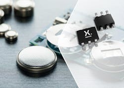
Nexperia added two new ideal-diode ICs to its portfolio of power devices. The NID5100 is suitable for standard industrial and consumer applications, while the NID5100-Q100 has been qualified for use in automotive applications.
Ideal diodes are MOSFET-based devices that offer much lower forward voltage drop than traditional diodes, and they make the perfect replacement option to standard diodes in systems where power efficiency is paramount. Applications that can benefit from the NID5100 ideal diodes include smart meters, fire/security sensors, battery-powered wearables, and automotive telematics units.
The NID5100 is a PMOS-based ideal diode—the gate voltage of an internal MOSFET regulates the “anode” to “cathode” voltage to be 8X to 10X lower than the forward voltage drop of similarly rated Schottky diodes. Besides the low forward drop, the MOSFET-based ideal diode also helps to reduce reverse DC leakage current by up to 100X compared to a typical Schottky diode.
Unlike other competitive ideal diodes, the NID5100 supports “OR-ing” of multiple power supplies while retaining reverse-polarity protection. It also provides ultra-fast response time for smooth power transfer. Other advantages include a forward regulation voltage of 31 mV (typ), the ability to handle forward current up to 1.5 A, and an automatic transition between OR-ed supplies.
The device operates within a voltage range of 1.2 to 5.5 V and has low current consumption, with a 3.3-V VIN shutdown current of just 170 nA and a quiescent current of 240 nA. The diode further includes reverse-voltage protection with an absolute maximum rating of −6 V and an output status indication (ST), making it a robust and efficient choice for power-management applications.
The NID5100 and NID5100-Q100 come in compact TSSP6/SOT363-2 leaded plastic packages measuring only 2.1 × 1.25 × 0.95 mm.
Learn more about Nexperia’s ideal diodes by clicking here.
Class-D Amp with Integrated Diagnostics Helps Designers Deliver Clear, Powerful In-Car Audio
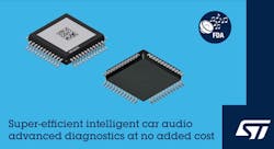
The HFA80A automotive-grade, analog-input, class-D audio amplifier, developed by STMicroelectronics, combines high efficiency, small size, and a low bill of materials, with load diagnostics optimized for automotive and native electromagnetic compatibility (EMC).
With its feedback-before-filter topology and 2-MHz nominal PWM frequency, the HFA80A lets designers optimize the output filter for the targeted performance and achieve a compact outline with small component values. Spread-spectrum operation simplifies meeting the mandatory CISPR 25 specification, with no additional EMC-specific filtering required.
The amplifier delivers clear and powerful listening experiences, driving up to 4x 49 W into 2-Ω speakers at 14.4 V, with typical harmonic distortion (THD) specified at 0.015% (1 W/4 Ω). Pure sound is assured, with low output noise and crosstalk as well as 80-dB power-supply rejection specified at 1 W/1 kHz with 4-Ω loads.
Flat frequency response up to 40kHz ensures generous bandwidth for high-resolution audio, which designers can extend to 80kHz by optimizing the filter. In addition, the HFA80A’s low-latency architecture enables it to handle performance-centric applications, such as noise cancelling, with ease
The automotive-specific diagnostics is based on a specially conceived noise-immune algorithm capable of detecting anomalous load conditions and variations. Features include independent DC and AC load detection for each channel, detection of short circuit on startup, and overcurrent protection with configurable thresholds. Further diagnostic checks include input-voltage DC-offset detection, output-current offset detection, and thermal protection with a choice of four different thermal warnings.
A dedicated, configurable pin signals the host microcontroller when new diagnostic information is available, which simplifies host communications and relieves CPU workload. An I2C-bus interface provides access to the device features and diagnostic data, and a backup mode lets the amplifier continue operating even if I2C control is lost. In addition, the HFA80A features a digital admittance meter (DAM) that eases development by helping engineers check the connected speaker characteristics without external measurement tools or sensors.
The HFA80A is available now in a compact 7- × 7-mm LQFP48L thermally enhanced package with exposed pads, from $4.80 for orders of 1,000 pieces.
For more information, click here.
New LCA Tool Facilitates Creation of Cost-Effective, Sustainable Products
EarthShift Global, a leader in lifecycle assessment (LCA) consulting and technology, has launched MatterPD, a unique software platform that approaches LCA through the lens of the product design process. The platform offers tools, approaches, and a price point designed to advance sustainability by giving product designers the ability to easily perform LCA modeling earlier in the process.
Conventional lifecycle analyses are often performed by looking backwards at an existing product’s environmental impact. In contrast, MatterPD software enables designers to monitor the impact of their design as it evolves, while presenting practical suggestions for improvements at every step along the way.
EarthShift’s new tool adds the dimension of sustainability to the design flow using a methodology called “underspecification.” It works with transparent uncertainty and imperfect data to model tens of thousands of possible scenarios for a given material category’s potential impact on the planet. This approach, developed in part at MIT’s Materials Research Laboratory, empowers better decision-making earlier in the design process.
“We know that 80% of a product’s environmental footprint can be cemented into a product during the design phase,” said Lise Laurin, founder and CEO of EarthShift Global. “MatterPD complements the design process by guiding designers to quickly understand and make better environmental decisions along the way when it comes to material selection and the material’s impact on climate, resource efficiency, and human health.”
EarthShift also overcomes the cost barriers that make most LCA software too expensive to use during the early stages of product design. It provides economical access by offering monthly pricing of $99/month. CEO Lauren explained that EarthShift Global’s pricing strategy is part of the company’s capacity building mission, “If we can get more people doing LCAs, and understanding the impact of the things we build, buy, and bury, that’s a good thing for the planet.”
EarthShift is an AutoDesk sustainability partner and is working to develop tools to integrate MatterPD with the popular product-design platform.
135- and 150-V MOSFETs Boost Efficiency in Drives and SMPS Applications
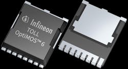
Infineon Technologies expanded its OptiMOS 6 MOSFET portfolio with 135- and 150-V product families. The devices are designed to meet the requirements of drives and switched-mode power-supply (SMPS) designs operating beyond the capabilities of the OptiMOS 6 120-V MOSFET series.
The family’s lower switching losses benefit applications like server SMPS, solar optimizers, high-power USB chargers, and telecom. Improved conduction losses benefit motor inverters in e-forklifts and light electric vehicles (LEVs).
Both new product families reduce on-state resistance (RDS(on)) up to 50% over earlier OptiMOS 5 devices, as well as a 20% reduction in figure of merit (FOM). As a result, they improve switching performance and excellent EMI behavior that enhances efficiency, power density, and reliability. The OptiMOS 6 series also features a faster and softer body diode that lowers QRR up to 59%, in addition to less overshoot and ringing.
The 135- and 150-V MOSFETs can be ordered now in a variety of packages: TO-220, D2PAK 3-pin, D2PAK 7-pin, TOLL, TOLG, TOLT, SuperSO8 5x6, and PQFN 3.3x3.3.
Eval Board Simplifies Design of High-Frequency Wireless-Power-Transfer Products Up to 6 W
A new evaluation board from Eggtronic lets engineers quickly develop and prototype ultra-efficient, low-component-count, wireless-power-transfer designs for low-power applications.
The WaveEgg Low-Power (LP) EVB is based on the company’s proprietary, high-frequency WaveEgg architecture, which optimizes performance and efficiency in high-performance power-converter and wireless-power-transmission systems. Well-suited to wirelessly charging and powering small, smart devices and IoT products, WaveEgg technology supports power transfers between 0.5 and 30 W and can work at extremely high frequencies (up to tens of megahertz, including ISM 6.78 - 13.56 - 27.12 MHz).
WaveEgg offers end-to-end efficiency that’s significantly higher than traditional systems, while reducing the overall bill of materials (BOM). Using the WaveEgg LP EVB, engineers will be able to create systems with high low-load to full-load efficiency using fewer components than standard class D, class E, class F, class Phi, and other resonant wireless-power-transfer solutions—including Qi- and Airfuel-based technologies.
“Wireless-power-transfer technology based on conventional designs has limitations in relation to size, bill of materials, and efficiency at reduced loads that limits its use for IoT and small smart devices,” said Igor Spinella, Eggtronic’s founder and CEO. “WaveEgg addresses the historical challenges of efficiency and component count for powers up to 30 W, and the WaveEgg 6W LP evaluation board provides a platform for engineers to quickly and easily realize practical and commercially viable low-power wireless designs.”
WaveEgg is based on Eggtronic’s EPIC (Eggtronic Power Integrated Controller) ICs. These ICs integrate a 32-bit RISC-V core and high-performance digital and analog peripherals. Their flexible internal structure supports control of both standard and proprietary power-conversion architectures. High efficiency over the whole load range is achieved through a proprietary design that achieves zero-voltage-switching (ZVS) and quasi-zero-current-switching (quasi-ZCS) on the transmission side and ZVS+ZCS on the receiving side.
With an output of 6 W and a switching frequency of 2 MHz, WaveEgg achieves an efficiency of 85%. The requirement for fewer components than conventional designs further contributes to efficiency by reducing losses from non-ideal component behavior. Additional component-count reduction is possible for battery-charging applications—the receiver can charge a battery through a step-down converter implementing a CC/CV-mode algorithm, eliminating the need for a battery-charger controller.
For more, click these links about Eggtronic’s wireless power technology and its EPIC1AQW01 and EPIC1AQW02 ICs.
Compact, AEC-Q101 Qualified N-Channel MOSFETs Offer High Efficiency and Reliability
Several N-channel automotive-grade MOSFETs unveiled by ROHM Semiconductor (RF9x120BKFRA / RQ3xxx0BxFRA / RD3x0xxBKHRB), which feature low on-resistance (RDS(on)), are well-suited for applications that include including motors for doors and seat positioning, as well as LED headlights.
The new components were developed in response to the growing demand for automotive electrical products that deliver power efficiency to optimize fuel and electricity consumption. Especially for MOSFETs essential for switching applications in automotive systems, there’s a growing requirement for lower RDS(on) to minimize loss and heat generation.
Offered in voltage ratings of 40, 60, and 100 V, the new products incorporate a split-gate structure to achieve low RDS(on), contributing to higher-efficiency operation in automotive applications. All models are qualified under the AEC-Q101 automotive reliability standard, guaranteeing exceptional high reliability.
Applications Include:
- Vehicle motors (e.g., doors, seat positioning, power windows)
- LED headlights
- Car infotainment/displays
- Advanced driver-assistance systems (ADAS)
The devices are available in three package styles. For space-constrained applications like ADAS, there’s the compact DFN2020Y7LSAA (2.0 × 2.0 mm) and HSMT8AG (3.3 × 3.3 mm) packages. For automotive power applications, the widely used TO-252 (DPAK) package (6.6 × 10.0 mm) is also available. In addition, ROHM further enhanced mounting reliability by utilizing wettable flank technology for the DFN2020Y7LSAA package and gull-wing leads for the TO-252 package.
AEC-Q200-Compliant, Automotive-Grade Multilayered Varistors
Bourns Inc.’s Model BVRA Series AEC-Q200-compliant, automotive-grade multilayered varistors feature excellent transient energy absorption thanks to improved energy volume distribution and power dissipation. Designed specifically for use in automotive circuits requiring surge protection, the new series can also be applied to protect other integrated circuits and components such as power supplies, entertainment electronics, or CAN, LIN, and FlexRay-based modules.
The Model BVRA Series is available with working voltages from 5.5 to 85 V DC and provides a quick response time of less than 0.5 ns to help ensure prompt energy diversion during transient events. Offered in a range of compact 0402, 0603, 0805, and 1206 SMD packages, the varistors have an insulator overcoat designed to help enhance efficiency and streamline integration. In addition, these models meet the IEC 61000-4-5 standard and deliver stable leakage current for a high-reliability, consistent overvoltage protection solution.
The Bourns Model BVRA varistor series, available now, is RoHS-compliant and lead-free. For more detailed product information, click here.
GaN Power ICs Integrate Autonomous EMI Control and Lossless Sensing
The GaNSlim family from Navitas Semiconductor is a new generation of highly integrated GaN power ICs that will further simplify and speed the development of small-form-factor, high-power-density applications by offering a high level of integration and thermal performance.
GaNSlim simplifies system design by integrating drive, control, and protection, with integrated EMI control and lossless current sensing, all within a high thermal performance proprietary DPAK-4L package. In addition, with an ultra-low startup current below 10 µA, GaNSlim devices are compatible with industry-standard SOT23-6 controllers and eliminate HV startup.
The lossless current sensing eliminates the need for discrete resistors and optimize system efficiency and reliability. Overtemperature protection ensures system robustness and auto sleep-mode increases light and no-load efficiency. Autonomous turn-on/off slew rate control maximizes efficiency and power density while reducing external component count, system cost, and EMI.
GaNSlim features a patented, 4-pin, high-thermal-performance, low-profile, low-inductance, DPAK package. This package enables 7°C lower temperature operation versus conventional alternatives, supporting high-power-density designs with ratings up to 500 W. Target applications include chargers for mobile devices and laptops, TV power supplies, lighting, etc.
Devices in the NV614x GaNSlim family are rated at 700 V with RDS(ON) ratings from 120 to 330 mΩ. They’re available in versions optimized for both isolated and non-isolated topologies.
A series of demo boards for GaNSlim devices allow for rapid evaluation and selection of the optimum device for applications such as QR flyback, single-stage PFC, boost PFC plus QR flyback, and TV power-supply designs.
Solar-Powered Desalination System Requires No Extra Batteries
MIT engineers have successfully completed large-scale field trials of a new type of battery-free solar-powered desalination system: It quickly adjusts its output according to the available solar energy.
Because the system can quickly react to subtle changes in sunlight, it’s able to make efficient use of the utility of solar energy, producing large quantities of clean water despite variations in sunlight throughout the day. In contrast to other solar-driven desalination designs, the MIT system requires no extra batteries for energy storage, nor a supplemental power supply, such as from the grid.
According to MIT Researcher Dr. Amos G Winter, the system is geared toward desalinating brackish groundwater—a salty source of water found in underground reservoirs that’s more prevalent than fresh groundwater resources. The researchers see brackish groundwater as a huge untapped source of potential drinking water, particularly as reserves of fresh water are stressed in parts of the world.
Pump and Flow
The new system builds on a previous design, which Winter and his colleagues, including former MIT postdoc Wei He, reported earlier this year. That system aimed to desalinate water through “flexible batch electrodialysis,” a process that uses an electric field to draw out salt ions as water is pumped through a stack of ion-exchange membranes. This process can run efficiently on power sources with widely varying outputs (such as the sun). Until recently, most conventional desalinization systems have relied on reverse osmosis systems, which tend to require operation at a steady power level.
In their previous design, the team built an electrodialysis system consisting of water pumps, an ion-exchange membrane stack, and a solar-panel array. The innovation in this system was a model-based control system that used sensor readings to predict the optimal rate at which to pump water through the stack in near-real-time. Thanks to this innovation, the earlier system was able to use an average of 77% of the available electrical energy produced by the solar panels
Solar Commands
In their latest project, the researchers looked to eliminate the need for batteries by shortening the system’s control-loop response time to a fraction of a second. The new system can adjust its desalination output in response to the available solar power at a rate of three to five times per second. This eliminates the need for batteries that would usually be needed to make up for any lag in power.
The engineers incorporated the new control strategy into a fully automated system that they sized to desalinate brackish groundwater at a daily volume of up to 5,000 liters per day, or enough to supply a community of about 2,000 people. During a six-month test, conducted at the Brackish Groundwater National Research Facility in Alamogordo, New Mexico, the system was able to utilize an average of over 94% of the solar panel’s output for desalination.
The engineers plan to further test and scale up the system in hopes of supplying larger communities, and even whole municipalities, with low-cost, fully sun-driven drinking water.
The full details of the technology behind the new system are available in a paper written by Bessette, Winter, and staff engineer Shane Pratt that will appear in Nature Water.
Read more articles in the This Week in PowerBites Library Series.
About the Author
Lee Goldberg
Contributing Editor
Lee Goldberg is a self-identified “Recovering Engineer,” Maker/Hacker, Green-Tech Maven, Aviator, Gadfly, and Geek Dad. He spent the first 18 years of his career helping design microprocessors, embedded systems, renewable energy applications, and the occasional interplanetary spacecraft. After trading his ‘scope and soldering iron for a keyboard and a second career as a tech journalist, he’s spent the next two decades at several print and online engineering publications.
Lee’s current focus is power electronics, especially the technologies involved with energy efficiency, energy management, and renewable energy. This dovetails with his coverage of sustainable technologies and various environmental and social issues within the engineering community that he began in 1996. Lee also covers 3D printers, open-source hardware, and other Maker/Hacker technologies.
Lee holds a BSEE in Electrical Engineering from Thomas Edison College, and participated in a colloquium on technology, society, and the environment at Goddard College’s Institute for Social Ecology. His book, “Green Electronics/Green Bottom Line - A Commonsense Guide To Environmentally Responsible Engineering and Management,” was published by Newnes Press.
Lee, his wife Catherine, and his daughter Anwyn currently reside in the outskirts of Princeton N.J., where they masquerade as a typical suburban family.
Lee also writes the regular PowerBites series.


