Ultra-Thin Silicon Wafers Wring More from Power Electronics
Modern chips are manufactured on slabs of silicon less than a millimeter thick. But semiconductor companies try to slice these silicon wafers thinner and thinner to squeeze more performance out of existing designs.
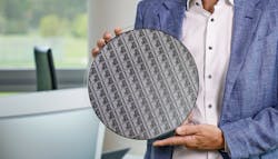
Infineon Technologies recently revealed what it called the thinnest silicon power wafers ever mass-produced in a bid to boost the power efficiency, power density, and reliability of its power-conversion solutions, specifically DC-DC converters that feed the AI chips in data centers. The newly produced power wafer is 20 µm thick, which is half as thick as current state-of-the-art wafers for power semiconductors that typically measure 40 to 60 µm.
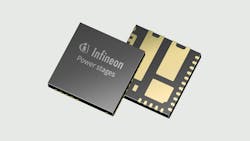
The company said it’s applying the innovation to its Integrated Smart Power Stages, which are widely used as 12-V DC-DC converters in data centers and other low-voltage domains. They provide the local power rails running into CPUs, GPUs, SoCs, and even power-hungry AI chips.
By halving the thickness of the silicon wafer, Infineon claims it can reduce substrate resistance by 50% compared to traditional wafers and curtail power losses by 15% at the system level. The slab of silicon features a diameter of 300 mm, which is the industry standard.
Infineon is trying to address the AI power dilemma because it could pay huge dividends over the long term. While a traditional server is comprised of power chips worth $65 to $80, Infineon estimates the latest servers for AI contain chips totaling $850 to $1,800, depending on the architecture. Adam White, Infineon’s president of the power and sensor systems, said in a statement: “As energy demand for AI data centers is rising significantly, power efficiency gains more and more importance.”
The plan is to apply the technology to more of its sub-40-V power electronics over time, including in power-supply designs for consumer, computing, and motor-control systems. At the current pace, Infineon executives said to expect the replacement of the standard silicon wafers used in its low-voltage power converters within three years or so.
The company will display the new ultra-thin silicon wafer for the first time at the electronica 2024 trade show in Munich.
Why Power Transistors Could Use Thinner Cuts of Silicon
According to Infineon, it will use the new ultra-thin power technology to boost its OptiMOS trench power MOSFETs.
In trench power MOSFETs, the current travels vertically from the drain of the power transistor on the front side of the silicon wafer to the source on the other side. If the current is forced to travel long distances through the channel, it requires more power, produces heat, and reduces bandwidth due to the resistance it encounters in the silicon. The length of the current path comes down to the thickness of the silicon substrate, said Richard Kuncic, head of the power systems business at Infineon.
The resistance present in the silicon substrate is dominant. “When thinking of a 15-V MOSFET, the portion of the substrate resistance already surpasses 50% of the total resistance,” said Kuncic. “Reducing the thickness from 40 to 60 µm down to 20 µm directly leads to a significant reduction in the total resistive losses, which translates to power losses (I2R).” These are the dominant power losses at higher load currents, which aren’t unusual in the latest AI chips, which burn through 1000 W or more.
>> Check out this TechXchange for similar articles and videos
For future generations of 10- to 12-V power MOSFETs, the new ultra-thin power wafers enable up to 40% less on-resistance (RDS(on)) than traditional silicon wafers. Thus, they can handle higher currents in physically smaller dies without being hampered by heat.
The ultra-thin power wafers also bring the ground plane closer to the back side of the power MOSFET, unlocking faster switching frequencies and efficiency. In general, thinner cuts of silicon also have superior heat dissipation, which is crucial for performance and longevity.
But slicing these slabs of silicon as thin as 20 µm presents challenges regarding the fragility and durability of the power devices. One of the tradeoffs with the new ultra-thin power technology is that the metal stacked on the surface of the silicon wafer to produce the power MOSFET is thicker than the underlying silicon wafer. That made it more difficult to do everything from handling and processing the ultra-thin silicon chips to packaging them, noted Kuncic.
Infineon's engineers solved the issue by creating a more innovative way of grinding down the ultra-thin silicon chips to reduce the risk of wafer breakage. It overcame several other technical and production-related hurdles, such as wafer bow and wafer separation, to ensure stability and robustness. The durability makes a difference in the backend assembly and packaging of the power chips. Kuncic said improvements were made to its laser cut alignment, too.
Furthermore, Infineon made sure these ultra-thin silicon wafers could be seamlessly integrated into its 300-mm production lines without incurring additional manufacturing complexity, ensuring high yield and quality control.
“Infineon has mastered the mechanical challenges to enable this technology,” Kuncic told Electronic Design.
Ultra-Thin Power Wafers: A Boon to AI Power Regulation
However, in the world of power electronics, a wafer is only as advanced as the chips manufactured on top of it.
Infineon said it would use the ultra-thin wafer technology to upgrade its Integrated Smart Power Stages for the next generation of GPU and AI chips in data centers. These DC-DC converters step down 5-, 12-, or 48-V power rails to the core voltages used by AI chips, which currently range from around 1.8 to 0.8 V. These buck converters provision the local power rails routing into the processor, so they must be placed as close as possible to avoid static and dynamic voltage drops and limit power losses stemming from resistance on the PCB.
When paired with optimizations to Infineon's chip designs, gate drivers, and power transistors, the ultra-thin wafer technology enables efficiency gains of up to 3% at 50 A, said the company.
The smart power stages also serve as the backbone of its high-performance, multi-phase voltage-regulator modules (VRMs), which can sling even larger amounts of current—in excess of 100 A each. As the latest GPUs and other AI chips become more power-hungry, these power modules can come together in multiphase DC-DC converters to supply high currents of more than 1,000 A over the last inch of the power-delivery network (PDN).
The ultra-thin wafer technology is also a boon to vertical power delivery designs: In these situations, the DC-DC converter is placed directly under the GPUs or other AI processors, feeding power a shorter distance up through the PCB, reducing lateral power losses and heat. These voltage regulators are based on its vertical trench power MOSFETs, so it pays dividends to place them directly under the processor to keep the power flowing in the same direction.
The ultra-thin wafer technology, which has been qualified, is sampling in power stages with early customers.
Si, GaN, and SiC: The Three Pillars of Power Electronics
This breakthrough bolsters Infineon’s focus on mastering all leading power semiconductor materials, including silicon carbide (SiC) and gallium nitride (GaN), which are more relevant at high voltages when compared to silicon (Si).
“The new ultra-thin wafer technology drives our ambition to power different AI server configurations from grid to core in the most energy-efficient way,” said Infineon’s White. The company recently rolled out a reference design for a power-supply unit (PSU) that leverages Si, SiC, and GaN power devices in a hybrid architecture aimed at AI. The PSU steps down AC voltages as high as 230 V to DC bus voltages of 12 or 48 V that travel over the PCB to the buck regulators clustered around the AI silicon.
The new announcement comes after Infineon pioneered the world’s first 300-mm power wafer based on GaN last month, and it opened the doors to the world’s largest 200-mm semiconductor fab for SiC power devices.
>> Check out this TechXchange for similar articles and videos
About the Author
James Morra
Senior Editor
James Morra is the senior editor for Electronic Design, covering the semiconductor industry and new technology trends, with a focus on power electronics and power management. He also reports on the business behind electrical engineering, including the electronics supply chain. He joined Electronic Design in 2015 and is based in Chicago, Illinois.


