Enhance Power-Delivery Networks with High-Bandwidth Integrated Voltage Regulators
What you’ll learn:
- Why the power-delivery network is critical in modern power electronics.
- How integrated voltage regulators can improve the PDN and simplify the PCB design.
- How IVRs improve power delivery to processors and other high-speed digital components compared to traditional voltage regulators.
With advancement in technology, processors and other high-speed digital components such as CPUs, GPUs, ASICs, and FPGAs demand increasingly higher power, which means voltage regulators need to be able to dynamically supply current to the load. Lower voltage requirements, high current, and faster transients with tighter voltage windows lead to more emphasis on the performance of the PCB traces that carry the current to the processor.
The power-delivery network (PDN) in between the voltage regulator and the load greatly impacts the ability of the regulator to source current. A PDN is a combination of passive components (typically capacitors) and the routes (the metal layers and vias) connecting the output of the voltage regulator to the input of the load. It can be represented by a circuit of parasitic resistive, capacitive, and inductive components.
High-bandwidth integrated voltage regulators (IVRs) can be placed closer to the processor than traditional voltage regulators, simplifying the PDN and allowing for more capability to quickly respond to dynamic load requirements. IVRs enable the user to place the regulator below the processor, simplifying the PDN and reducing the power loss from the resistance in the trace.
Vertical power delivery improves the power-delivery performance to the load. It also reduces the PCB complexity by allowing for fewer PCB layers and more space on the top side of the PCB for other components. The key differentiator of IVRs is that they integrate input and output capacitors into the die to further reduce the number of components on the PCB. High-frequency switching increases the bandwidth and further reduces the need for output capacitors. Moreover, it improves the load transient performance and allows for a flatter output impedance curve.
>>Download the PDF of this article
PCB Impedance and PDN Target Impedance Challenges
In modern, high-performance applications such as CPUs, GPUs, and FPGAs, the ability to source power to the load while meeting its power requirements is becoming ever-more critical. This is also the case regarding proper PCB design, to ensure that the power requirements of the load can be met.
The PDN between the voltage regulator and the load has a large impact on the ability of the regulator to source current. The PDN is made up of the capacitors, PCB traces, layers, and vias that are used to connect the output of the regulator to the SoC load (Fig. 1).
The PDN’s parasitic resistance increases the power loss of the power circuit, which decreases the system efficiency and leads to a voltage drop in between the voltage regulator and the load. Larger parasitic resistance requires the voltage regulator to regulate a higher output voltage to meet the voltage requirement at the load. This leads to larger power loss; therefore, the parasitic resistance in the PDN must be minimized. Larger inductance in the PDN prevents the regulator from being able to source high-frequency load transients.
The target impedance must be met by the PDN to enable the voltage regulator to supply power to the load without violating any power requirements. The voltage droop across a PDN due to a load transient can be determined by the following equation:
Keeping the ZPDN small also allows the user to program the output voltage of their regulator to a lower value, saving system power. ZPDN can be decreased by carefully designing the PCB. The impedance of a PCB trace is proportional to its parasitic inductance and inversely proportional to its parasitic capacitance.
To reduce the PDN impedance, a large capacitor bank is often required at the output of the voltage regulator along with decoupling capacitors underneath the SoC. The added capacitance from the capacitor bank increases the denominator of the above equation, reducing the overall impedance. The capacitor bank underneath the SoC requires that the voltage regulator be placed to the side of the SoC, meaning that the current must travel laterally, increasing the parasitic inductance and resistance (Fig. 2).
Voltage Regulator Output Impedance
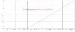
A voltage regulator’s output impedance can be represented by a resistor in series with an inductor. The resistor represents the output load regulation. The inductor represents the bandwidth of the regulator, and therefore how well the regulator can respond to transient load conditions. Typically, the equivalent inductance is about an order of magnitude lower than the power-stage inductor, which is chosen based on the switching frequency of the circuit, the input voltage, output voltage, and desired inductor current ripple. Figure 3 shows the output impedance of a standard DC-DC buck converter.
Capacitors can be used to compensate for the equivalent inductance of the voltage regulator to create a flat impedance across a wide frequency range.
To determine the impedance spec that a design must target, the engineer must know their maximum load step and the allowable voltage droop. For example, if the engineer has a maximum load step of 6 A and a maximum voltage deviation of 50 mV, then the target impedance can be calculated with the following equation:
A standard voltage regulator with a 1-MHz switching frequency has a bandwidth of 100 kHz, leading to a transient response time of 1 µs. Using this control-loop bandwidth and the above target PDN impedance, the output inductance of our traditional voltage regulator must be:
A standard switching regulator running in the 1-MHz range with a 200- to 500-nH main inductor is appropriate to achieve this output inductance. To compensate for the output inductance of the regulator to keep the impedance as flat as possible, capacitors with lower inductance (ESL) must be used, where capacitance is C1 > C2 > C3 and ESLC1 > ESLC2 > ESLC3.
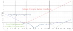
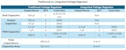
The ESL of a ceramic capacitor is typically proportional to its case size. Choosing multiple different capacitors in different case sizes allows the engineer to create a flat impedance across a wider frequency range. This example uses a 180-µF bulk capacitor, 2x 100-µF 0805 ceramic capacitors, 2x 47-µF 0603 ceramic capacitors, 1x 10-µF 0402 ceramic capacitor, 2x 2.2-µF 0402 ceramic capacitors, 1x 1.0-µF 0201 ceramic capacitor, and 3x EC1001 200-nF silicon capacitors. Utilizing these capacitance values leads to the impedance curve shown in Figure 4, which meets our target impedance up to 168 MHz.
PDN Improvements Due to High-Frequency IVRs
An IVR is a type of voltage regulator that leverages small process geometries, high switching frequencies, and increased integration to place the regulator as close as possible to the load. In general, IVRs operate up to 100X the switching frequency of a traditional DC-DC voltage regulator, often in the 10- to 100-MHz region.
Operating at a higher switching frequency increases the loop bandwidth of the regulator and reduces the need for large capacitor banks to meet transient requirements. In addition, IVRs typically use multiple phases to further increase the loop bandwidth and mitigate the output capacitance requirements.
One example of an IVR is the EP7123 from Empower Semiconductor, which delivers 6 A using four phases and has a bandwidth around 8 MHz. To achieve the target PDN impedance discussed above, the IVR output inductance must be the following:
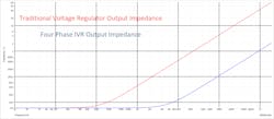
This is 100X smaller than the traditional voltage regulator’s equivalent output inductance. Figure 5 depicts an output impedance comparison of the traditional voltage regulator shown earlier to a multiphase IVR.
The impedance plot demonstrates that the IVR has much lower output inductance than the traditional voltage regulator, which causes the impedance to begin to rise at a much higher frequency. Using multiple phases for the IVR puts the output inductances in parallel and further lowers the impedance. The lower output impedance of the multiphase IVR enables the designer to cut down the number of capacitors placed in the PDN to meet the target impedance.
These differences significantly improve the regulator response time. A standard switching regulator has a bandwidth of around 100 kHz and a response time of 10 µs. In comparison, a multiphase IVR can have a bandwidth of over 10 MHz and a response time of 100 ns.
An IVR can also achieve a solution height below 0.8 mm, which is much lower than a traditional voltage regulator solution. Lower solution height allows for the IVR to be placed on the back side of the PCB, directly beneath the load (Fig. 6).
Enabling vertical power delivery simplifies the PDN from the IVR to the load, lowering the impedance of the delivery path. On top of that, the EP7123 integrates output capacitors, reducing the need to place these components externally. All of this lowers the overall impedance, the need for bulk capacitors, and the power loss due to trace resistance.
The combined effect of the high-bandwidth IVR and its vertical delivery placement is illustrated in the revised PDN in Figure 7. The most striking differences are the wholesale removal of the bulk capacitors and the impedance from the output of the voltage regulators to the previously required decoupling capacitors.
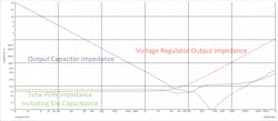
Due to the higher bandwidth, much fewer capacitors are required on the path between the IVR and the SoC to meet the target impedance for the PDN. Using a 1x 2.2-µF 0402 capacitor, 2x 1-µF 0201, and 3x EC1001 215-nF ECAPs forms the PDN shown in Figure 8.
Employing a high-frequency IVR such as the EP7123, the same target impedance as the previous example was met with 100X lower capacitance and 12X smaller area. This enables cost savings thanks to a lower BOM count and shrinks the solution size of their power circuitry on the PCB.
The capacitors used for the IVR and for the traditional voltage regulator can be found in the table. The IVR requires much fewer capacitors, as well as capacitors with smaller case sizes. The high-bandwidth regulation allows for the removal of the large bulk capacitors used for the traditional regulator, limiting the capacitors needed to improve the PDN to only a couple of 0402 and 0201 capacitors to meet the target impedance. This helps reduce the PCB complexity, solution size, BOM count, and therefore the final cost of the design.
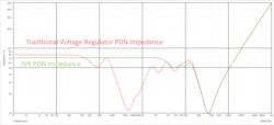
In addition to reducing the number of required capacitors, the IVR impedance is also flatter and more consistent across a wider frequency range (2 MHz) compared to the traditional regulator (40 kHz) shown in Figure 9, without unwanted resonances that can lead to unstable behavior. These resonances could cause unstable behavior on the power supply; it’s ideal to be able to reduce them where possible. Overall, using an IVR such as the EP7123 leads to more predictable behavior from the power supply while also enabling a simpler design.
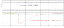
The benefit of having the flatter impedance curve over frequency is clearly evidenced by the transient performance shown in Figure 10. The simulation models the voltage regulators as simple output impedance models. Hence, it’s only to be used to compare the relative differences in droop between a traditional regulator versus an IVR.
The lower output inductance of the IVR leads to a faster response to the load step and a lower droop on the output voltage. A lower output-voltage droop enables the engineer to set the output voltage lower while still meeting the minimum output voltage requirements of their system. This reduces static power consumption of the SoC and allows for a wider margin to the maximum allowable voltage.
With the ultra-fast recovery (<1 µs vs. >15 µs), the SoC can avoid mitigation strategies such as clock scaling or clock stretching and operate at its full potential. The flat frequency response also removes unwanted resonances, resulting in a cleaner transient response without inductive spikes. Overall, the high-frequency IVR enables a simpler design with improved performance over the traditional voltage regulator designs.
Optimizing the Power-Deliver Network with IVRs
In modern electronics, loads such as FPGAs, SoCs, and CPUs need a PDN with a low impedance and flat frequency response so that the voltage regulator can adequately source dynamic loads. Traditional voltage regulators require many bulk capacitors, bypass capacitors, and local high-frequency capacitors to compensate for the higher output impedance of the regulator (high output impedance), parasitic inductances in the PCB, and the capacitors’ ESLs.
Despite all of the capacitors added to improve the PDN, undesired resonances can still occur to cause oscillations on the power supply, and the slow recovery to a dynamic load step can’t be avoided.
High-frequency IVRs such as the EP7123 from Empower Semiconductor can be used to optimize the PDN to remove the unwanted oscillations. IVRs can typically be placed directly underneath the load, which simplifies the PDN and reduces power loss across the PCB traces and vias. IVRs integrate input and output capacitors, which reduces the number of components on the PCB.
A higher switching frequency compared to a traditional voltage regulator provides a low impedance over a wider bandwidth, requiring much fewer output capacitors on the PCB. This allows for a flatter output impedance over frequency (no undesirable peaks and valleys).
Vertical power delivery leads to fewer PCB layers, reducing PCB complexity. The placement under the load helps to free PCB space on the top layer, which can be used to place memory or other components that can’t be placed on the bottom layer.
Overall, IVRs make it possible for the designer to significantly improve power integrity while also reducing the number of components.
References
1. Peterson, Zachariah. "What Target Impedance Should You Use in Your PDN?" Altium, 6 Jul. 2021,
2. Bruening, Ralf. "What PDN Target Impedance Means for PCB Designers," Zuken.
3. Sandler, Steve, et al. "Power Distribution Network (PDN) Impedance and Target Impedance," EDI Con.
4. "EP7123 Product Brief," Empower Semiconductor.
>>Download the PDF of this article
About the Author

Ryan Marquiss
Staff Product Marketing Engineer, Empower Semiconductor
Ryan Marquiss is a Staff Product Marketing Engineer at Empower Semiconductor, where he works on integrated voltage regulators and silicon capacitor technology. Previously, he spent seven years working as an Applications Engineer within the semiconductor industry, primarily on multiphase buck converters and other power-management integrated circuits. Ryan holds a Bachelor of Science in Electrical Engineering from the University of California, Davis.
Voice Your Opinion!
To join the conversation, and become an exclusive member of Electronic Design, create an account today!

Leaders relevant to this article:


