Pulsed RF Power for Angstrom-Scale Processes
What you’ll learn:
- Challenges like higher selectivity and precise etching are critical for angstrom-scale IC production.
- Advanced RF pulsing and plasma control enhance precision in sub-nanometer processes.
- New impedance-matching tech improves process stability and supports angstrom-level manufacturing.
As the semiconductor industry enters the Angstrom Era, with 2-nm process nodes nearing mass production, new challenges in precision and process control emerge. Advances in RF power delivery, including RF pulsing and direct match-generator synchronization, are critical to overcoming these challenges and pushing chip manufacturing into sub-nanometer scales.
Propelled by the relentless pursuit of smaller, faster, more efficient chips, the semiconductor industry is approaching an inflection point, manufacturing at sub-nanometer—or angstrom (Å)—scale geometries. Several leading companies in the industry will enter mass production for their 2-nm processes next year, just four years since the first such chips were fabricated in 2021.
With 1 Å equal to 10-10 m, or roughly half a silicon atom, even the smallest of variations in process conditions can lead to significant deviations in feature precision, impacting device performance, quality and yield. As a result, process requirements are becoming ever-more stringent.
6 Key Challenges for Angstrom-Era Fabrication
There are many challenges to overcome as we reach this inflection point, including:
- Higher selectivity: As feature size shrinks, so does given tolerance for the ratio of film and substrate etch rates (or the film and photoresist and other materials used as a mask) with which the processes need to interact with, or remove, one material without impacting another.
- Anisotropic etching: This is the directional, preferential removal of material along a specific axis during the etching process. Ensuring the vertical etch rate greatly exceeds the lateral rate enables the fabrication of smaller, denser features.
- Critical dimension control: To allow for yields at commercial levels, the process needs to be exact when it comes to the smallest features on the semiconductor device.
- Plasma-induced damage: Plasma etching and deposition can cause damage to the underlying materials if not carefully controlled. Again, processes manufacturing smaller features have smaller margins of error.
- Throughput: Manufacturers need to accommodate ever-tighter tolerances, but they also need to achieve this with high yields, at speed. As we have seen with 2-nm processes, this shift from proof of concept to commercial-volume manufacturing can take many years.
- Repeatability: Processes should run the same and yield the same results while conditions of control parameters are kept in requested tolerances.
To manage these challenges and reach mass production of Angstrom Era chips, systems have evolved to ensure tighter control of the plasma in etch and deposition processes.
RF Pulsing: Improving Plasma Control for Precision in Sub-Nanometer Processes
Over many decades, plasma power delivery has evolved alongside semiconductor devices to improve etch uniformity. To achieve angstrom-scale geometries, it will be essential to generate plasmas with tighter control of ion energy magnitudes and precise and tight ion energy distribution.>>Download the PDF of this article
Continuous-wave (CW) power delivery doesn’t allow for the flexible ranges of plasma operating conditions, nor the shorter process steps or the faster transitions that the new era demands. This can only be achieved through instantaneous adjustments in RF power and frequency, using pulses to precisely achieve the desired plasma characteristics across step-to-step process chemistry changes.
Both computation investigations and real-world experimental studies show how this pulsing of the RF power’s low- and high-power states increases the plasma processing flexibility: It enlarges the range of operating conditions for stable plasma operation.
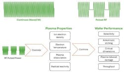
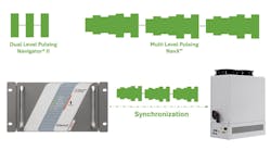
By varying the pulse frequency and duty cycle (the ratio of pulse on-time to total pulse duration), the RF generator provides additional “tuning knobs” (Fig. 1). These can control primary plasma properties such as ion/electron densities, the ion/neutral flux ratio, plasma dissociation, and plasma potential to help with the critical requirements of shrinking device sizes.The latest generation of RF generators provides multi-level pulsing with exceptionally quick transition times for exacting precise process control. This enables plasma characteristic customization for precise material removal during etch processes and controlled deposition in film growth. The speed and configurability can be seen in Figure 2.
In addition, this pulsed RF method of plasma ignition and maintenance reduces the heat on (and therefore damage to) the substrate during the off phase. It also enables dynamic optimization that lets specific pulse parameters be used at each stage of the fabrication, with flexibility and control over evolving requirements. On top of that, this targeted energy delivery achieves the etching/deposition with a lower power consumption versus continuous-wave RF.
Impedance-Matching Technology: Improving Plasma Stability and Yield
The move to multilevel pulsing requires such synchronization to allow for extremely fast impedance matching, leading to a new generation of matching networks. These networks enable optimal amplification settings to be less conservative than before and provide greater flexibility at each process step.
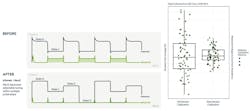
By better optimizing hardware response speeds in pulse sequences, it’s possible to maximize power transfer and reduce reflected power. The best networks also decrease tune-point dithering, use scalable pulse tune states for new energy regimes, and utilize more exacting sensor calibrations that minimize unit-to-unit deviation.
As an example, consider Advanced Energy’s third-generation impedance-matching network called NavX. This system can measure power delivery in real-time and directly link to the eVerest generator. Its proprietary Advanced Selectable Tuning and Velocity Tuning algorithms optimize response speeds for pulse sequences, while faster tuning and a wider impedance range is achieved via a ±10% frequency span. In addition, the use of intermodulation-distortion (IMD) immunity maintains tuning accuracy in multifrequency applications (Fig. 4).
Conclusion: Advancing Toward Sub-Nanometer Manufacturing with RF Innovations
With the continuing miniaturization of chips, even the smallest of variations in process conditions can lead to significant deviations in feature sizes, which impacts device performance, quality, and yield. Tighter control of the plasma used for the etching and deposition process is therefore essential.
Evolutions in RF plasma generators and impedance-matching networks is essential, with faster tuning and improved etch rates, as well as selective tuning for reduced instability/wafer scrap, proving crucial in enabling us to advance toward sub-nanometer processes.
>>Download the PDF of this article
About the Author

Niraja Bhalcharndra
Product Manager, Advanced Energy
Niraja Bhalcharndra works as a full-time RF Engineer for Advanced Energy. She has educational experience in CMOS technology, RF systems, RF amplifiers, wireless and communication, with hands-on experience in design and testing RF components.
Voice Your Opinion!
To join the conversation, and become an exclusive member of Electronic Design, create an account today!

Leaders relevant to this article:


