2024 PowerBest Winners: Passives, Packaging, and Applications
What you’ll learn:
- The quest for ever-higher power densities has encouraged the rise of breathtaking levels of active/passive device integration and cool-running packaging technology.
- Advanced packaging technologies are being used in combination with novel power-conversion architectures to offer extremely energy- and cost-efficient products for EVs, renewable power generation, and storage on other essential building blocks of the emerging green economy.
- Designing for sustainability is easier and more cost-effective than ever thanks to advances in lifecycle analysis (LCA) tools.
- New developments in embedded magnetics are changing the rules of engagement for delivering unprecedented levels of power density in power-supply designs.
onsemi All-SiC PIMs Lead to Smaller Fast-Charging Platforms with Bidirectional Charging
The series of EliteSiC power integrated modules (PIMs) developed by onsemi supports bidirectional charging capabilities for DC ultra-fast electric-vehicle (EV) chargers, as well as bidirectional charging applications for EVs and larger energy storage systems (ESS).
The silicon-carbide-based (SiC) solutions support key topologies such as multilevel T-type neutral point clamp (TNPC), half-bridge and full-bridge topologies for applications requiring 25 to 100 kW. Their high efficiency and simpler cooling mechanisms can reduce size by up to 40% and weight up to 52% compared to traditional silicon-based IGBT solutions.
Originally appeared in the January 2024 edition of PowerBites
TI Power Modules Use Advanced Magnetic Packaging to Slash Power-Solution Footprints
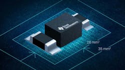
Texas Instruments’ TPSM828xxx series of power modules leverage the company’s proprietary MagPack integrated magnetic packaging technology to boost power density, enhance efficiency, and reduce electromagnetic interference (EMI) in industrial, enterprise, and communications applications.
The 3D package molding and packaging technology shrinks module size by up to 23% versus competing modules, while delivering power densities approaching 1 A per 1 mm2. (For more information, click here.)
Originally appeared in the July 2024 edition of PowerBites
Earthshift LCA Tool Makes it Easy and Cost-Effective to Design Sustainable Products
EarthShift Global launched MatterPD, a unique software platform that approaches lifecycle analysis (LCA) through the lens of the product design process. The platform offers tools, approaches, and a price point designed to advance sustainability by giving product designers the ability to easily perform LCA modeling earlier in the process.
In contrast to the workflows of conventional LCA tools, Earthshift’s interactive platform enables designers to monitor the impact of their design as it evolves, while presenting practical suggestions for improvements at every step along the way.
With subscriptions available for as little as $99/month, MatterPD makes it even easier for design teams to incorporate state-of-the-art LCA analysis into their workflow. CEO Lise Laurin said, “If we can get more people doing LCAs, and understanding the impact of the things we build, buy, and bury, that’s a good thing for the planet.”
For more information on MatterPD, including a free trial, click here.
Originally appeared in the October 2024 edition of PowerBites
Bourns Planar Signal BMS Transformer Boosts Reliability/Safety for EV, Energy Storage Systems
Bourns Inc.’s signal BMS transformer was the first device of its kind to employ a planar structure. This is significant because planar-style signal transformers have been introduced to increase design flexibility and robustness. They’re also known to deliver cost efficiency and reliability advantages over conventional wire-wound transformer designs due to their multilayer PCB isolation and full automation.
The transformer features a working voltage up to 1,000 V DC and superior clearance/creepage distance features, and it complies with Overvoltage Category II. For additional product information, click here.
Originally appeared in the January 2024 edition of PowerBites
SemiQ 1,200-V Full-Bridge SiC MOSFET Modules Target Solar Inverter, EV Charging Apps
SemiQ co-housed a pair of its QSiC 1,200-V SiC MOSFETs in a high-performance ceramic thermal package to create a full-bridge driver that offers near zero switching loss. The end result is improved efficiency and reduced heat dissipation that enables the use of smaller heatsinks in solar inverters, EV chargers, and other high-power applications.
Featuring a breakdown voltage exceeding 1,400 V, the QSiC modules can withstand high-temperature operation at Tj = 175°C with minimal RDS(on) shift across the entire temperature spectrum. To guarantee a stable gate threshold voltage and premium gate-oxide quality for each module, SemiQ conducts gate burn-in testing at the wafer level.
Originally appeared in the March 2024 edition of PowerBites
>>Check out our other 2024 PowerBest winners
About the Author
Lee Goldberg
Contributing Editor
Lee Goldberg is a self-identified “Recovering Engineer,” Maker/Hacker, Green-Tech Maven, Aviator, Gadfly, and Geek Dad. He spent the first 18 years of his career helping design microprocessors, embedded systems, renewable energy applications, and the occasional interplanetary spacecraft. After trading his ‘scope and soldering iron for a keyboard and a second career as a tech journalist, he’s spent the next two decades at several print and online engineering publications.
Lee’s current focus is power electronics, especially the technologies involved with energy efficiency, energy management, and renewable energy. This dovetails with his coverage of sustainable technologies and various environmental and social issues within the engineering community that he began in 1996. Lee also covers 3D printers, open-source hardware, and other Maker/Hacker technologies.
Lee holds a BSEE in Electrical Engineering from Thomas Edison College, and participated in a colloquium on technology, society, and the environment at Goddard College’s Institute for Social Ecology. His book, “Green Electronics/Green Bottom Line - A Commonsense Guide To Environmentally Responsible Engineering and Management,” was published by Newnes Press.
Lee, his wife Catherine, and his daughter Anwyn currently reside in the outskirts of Princeton N.J., where they masquerade as a typical suburban family.
Lee also writes the regular PowerBites series.
