Dynamically Testing WBG Power Semiconductors Down to the Die
Double-pulse testing will play a pivotal role in the future of power electronics. Power designers and system engineers rely on it to evaluate the switching characteristics of power semiconductors such as MOSFETs and IGBTs under dynamic conditions. By evaluating power losses and other metrics during switching, these tests enable engineers to optimize the efficiency and reliability of the latest power converters, inverters, and other power circuits.
Driving the adoption of double-pulse testing is its ability to evaluate power electronics under worst-case operating conditions early in the design process. That helps reduce the risk of unforeseen issues in the future.
However, dynamically testing power devices based on gallium nitride (GaN) and silicon carbide (SiC) presents distinct challenges due to the faster switching speeds of SiC MOSFETs and even higher frequencies of GaN power FETs. As a result, engineers working with these next-gen power semiconductors continue to face obstacles when attempting to reduce power losses.
Dynamic Measurement
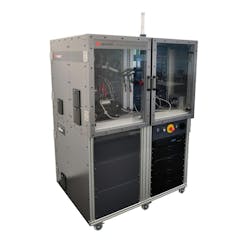
Keysight Technologies is trying to tackle the issue by giving engineers the ability to measure the dynamic characteristics of wide-bandgap (WBG) power semiconductor die before they’re packaged. Keysight said the test fixture is specifically designed to minimize parasitics that can impact the accuracy and reliability of double-pulse testing on bare dies, and it eliminates the need for soldering. The unit is compatible with the company’s double-pulse testers, including the PD1550A (see figure).
“With the introduction of the new WBG semiconductor bare chip evaluation method, we are helping the industry expedite the development of highly efficient and robust power semiconductor discrete devices and power modules,” said Thomas Goetzl, VP and GM of automotive and energy solutions at Keysight.
Power semiconductors based on SiC and GaN are core building blocks in everything from onboard chargers (OBCs) and traction inverters in electric vehicles to solar, wind, and other renewable-energy systems connected to the grid. They also have the potential to alleviate the rapidly growing power demands of data centers, which are driving the latest advances in AI. But they’re used in many different forms, including pre-packaged devices or power modules containing the bare semiconductor die.
>>Check out more of our APEC 2025 coverage
What is the Double-Pulse Test?
The double-pulse test (DPT) is the most widely adopted method for measuring the characteristics of these power semiconductors in hard-switching situations. It reveals valuable insights into the power device in dynamic conditions, giving engineers the ability to accurately gauge everything from energy losses during turn-on (Eon) and turn-off (Eoff) to current (di/dt) and voltage (dv/dt) slopes. The test can also measure reverse-recovery characteristics (Qrr) of the power device and the operation of the gate driver that controls it.
With it, power designers and systems engineers can improve the efficiency of power conversion. It also helps them identify potential performance issues early in the design process, resulting in more robust and reliable power designs.
A double-pulse test requires several pieces of equipment. A power supply or source-measurement unit (SMU) delivers the voltage, while the arbitrary function generator (AFG) or other testers output the gate-drive signals that switch the power device on and off, allowing engineers to assess how it performs under different current loads and at varying temperatures. The ability to supply accurate gate-drive signals—these are the “pulses” in double-pulse testing—is critical for conducting these tests.
By adjusting the turn-on and turn-off times, engineers can observe and analyze the switching waveforms of the power device. In most cases, a high-bandwidth mixed-signal oscilloscope is used to capture these high-speed signals, and it’s paired with several different probes to measure the gate and drain current of the power device as well as perform isolated high-side gate voltage measurements. That data is critical for understanding how the power device performs across a range of conditions.
In a typical setup, a pair of pre-packaged power devices are placed in a half-bridge topology on an evaluation board with gate drivers and current sensors. The PCB is specifically designed for the purpose of double-pulse testing.
Testing bare power semiconductors can give engineers a more complete understanding of the switching characteristics of power devices, said Keysight. But measuring the dynamic operation of a power transistor before packaging usually requires soldering directly onto the bare chip. This process is not only difficult, but it can also cause parasitics that impact the accuracy and reliability of the measurements, according to the company.
Minimizing Parasitics of Bare Power Devices
Keysight said it takes care of these challenges with its latest test system, which allows power device engineers and systems designers to perform dynamic characterization as soon as the chip is diced from a wafer. The system facilitates the fast and easy accommodation of bare power devices, said Keysight, supplying more than enough electrical contact for testing while keeping a small and fragile chip from arcing or being damaged.
The unique design of the test fixture eliminates the need for soldering directly to the power device or the placement of needle-shaped probes on top of it. That minimizes parasitics in the test circuit and produces clean measurement waveforms for fast-switching SiC and GaN power devices. The system has parasitic power-loop inductance of less than 10 nH. “Bare chip dynamic characterization, once regarded as almost impossible to do, is now possible with the extension to our power semiconductor test portfolio,” said Goetzl.
>>Check out more of our APEC 2025 coverage
About the Author
James Morra
Senior Editor
James Morra is the senior editor for Electronic Design, covering the semiconductor industry and new technology trends, with a focus on power electronics and power management. He also reports on the business behind electrical engineering, including the electronics supply chain. He joined Electronic Design in 2015 and is based in Chicago, Illinois.
Voice Your Opinion!
To join the conversation, and become an exclusive member of Electronic Design, create an account today!

Leaders relevant to this article:


