The Best Approaches for Improving Power Density
What you'll learn:
- How does higher switching frequency help increase power density?
- How can component selection help in achieving density goals?
- How can an optimized PCB layout improve power density?
- Further ways to improve thermal management of PCBs.
- Other important considerations in power-density design.
Higher power density is one of the keys to more competitive products that are able to deliver more, and better, features at a given competitive price point.
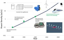
Designers know many tricks-of-the-trade and best practices. However, achieving higher power density can be challenging because many of those tried-and-true approaches end up conflicting or, at a minimum, being difficult to achieve in unison. And that’s the challenge—orchestrating all aspects of design to achieve the goal (see figure).
To boost a PCB's power density, you can primarily focus on:
- Increasing switching frequency in power converters to shrink passive components like inductors and capacitors.
- Utilizing advanced semiconductor technologies like gallium nitride (GaN) for faster switching speeds.
- Optimizing PCB layout for efficient heat dissipation.
- Integrating more components on a smaller footprint.
- Carefully designing thermal-management systems to handle the increased heat generated at higher power densities.
How Does Higher Switching Frequency Help Increase Power Density?
By operating power converters at higher switching frequencies, the size of passive components like inductors and capacitors can be significantly reduced, leading to a smaller overall footprint. Why? Because at higher frequencies, these components need to store less energy per switching cycle, enabling smaller physical sizes. When this is applied across a system, the net results can be significant size reduction.
>>Download the PDF of this article, and check out the Series Library for similar articles and videos
In particular, high switching frequencies allow for the use of smaller inductors and capacitors, which are among the largest components in a power converter. High switching frequency can enable faster response to load changes, requiring less output capacitance for stability. And, as noted, advancing semiconductor technologies like GaN enable very high switching frequencies, further enhancing power density potential.
How Can Component Selection Help in Achieving Density Goals?
Component selection is an obvious place to achieve better power density. In general, suppliers are following Moore’s Law and its corollaries, meaning newer designs usually provided better functionality for a given volume. This, of course, must usually be balanced against cost factors. But options abound.
In power devices, for example, MOSFETs—particularly those built on GaN—can deliver improved efficiency with fewer thermal-management challenges. GaN typically offers faster switching speeds and lower losses compared to traditional silicon, leading to greater power density in a smaller package.
Opting for smaller, high-density passive components like surface-mount capacitors and inductors can contribute to a smaller PCB area needed for power delivery and support better thermal dissipation. Similarly, using integrated circuits that combine multiple functions like power conversion and control circuitry into a single package minimizes component count and space requirements. These are areas seeing constant improvement, so it pays to explore both familiar and unfamiliar devices.
How Can an Optimized PCB Layout Improve Power Density?
A substantial portion of higher power density comes from implementing careful and strategic board layout. An optimized PCB layout can improve power density by:
- Minimizing power-distribution path lengths.
- Utilizing wide power planes to reduce resistance.
- Strategically placing decoupling capacitors near power pins.
- Using multiple vias to increase current carrying capacity.
- Carefully positioning high-power components to facilitate heat dissipation.
Strategic routing means carefully routing traces to minimize loop inductance and parasitic resistance, which can be significant sources of heat generation.
Basic common sense does help. Designers should think about how and where components with significant thermal output can be placed to optimize heat dissipation, as well as consider how bulky components could impede air flow. Multilayer PCBs may allow for some additional freedom in where components are placed, potentially improving cooling. Combined, these measures can effectively deliver more power in a smaller space with less voltage drop and heat generation.
Further Ways to Improve Thermal Management of PCBs
Thermal management has many facets. On the one hand, higher-density design can help eliminate some practices that might weed out inefficiency, but it may foment thermal issues. It also can lead to obvious problems. More devices in a given space not only generate more heat for a given unit of volume, but those devices can interfere with, for example, the efficient movement of air. This can generate higher component temperatures with a risk of increased component failure rates.
In addition, designers can look to incorporate effective heatsinks to manage heat generated by power components, especially when high power densities are involved. Implementing fans or other forced-air cooling mechanisms could also enhance heat dissipation. Furthermore, thermal vias (plated through-holes on a PCB designed to facilitate heat transfer from a hot component to other layers of the board) can help to conduct heat from the PCB surface to internal layers, where it would be better dissipated.
Some designers also incorporate relatively thick copper plates on the PCB for improved heat dissipation.
Some Other Important Considerations in Power-Density Design
- Switching losses: While increasing switching frequency can enhance power density, it also may lead to increased switching losses that need to be carefully managed through appropriate circuit design and component selection.
- EMI concerns: High switching frequencies can generate significant electromagnetic interference (EMI), requiring proper filtering and shielding techniques. Of course, dense designs could make it difficult to accommodate EMI filters. On the other hand, compact, economical layout not only reduces radiated emissions, it also tends to reduce reception of incoming EMI. It’s recommended to keep loops containing high di/dt (the rate of change of current over time) to a minimum.
- Design tradeoffs: Ultimately, almost every facet of increasing power density is about tradeoffs. Balancing the need for high power density with other factors like efficiency, cost, and reliability is crucial. All design factors must be considered more or less simultaneously, because each has an impact on the others. The reward can be a robust and very efficient end-product.
References
Understanding the Trade-offs and Technologies to Increase Power Density, Texas Instruments.
Achieving higher power density with good-old Si MOSFETs, Vicor.
>>Download the PDF of this article, and check out the Series Library for similar articles and videos
About the Author

Alan Earls
Contributing Editor
Voice Your Opinion!
To join the conversation, and become an exclusive member of Electronic Design, create an account today!

Leaders relevant to this article:


