Hysteretic-Mode Converters Demystified - Part 3: Regulator Stability
Three tools will be used to review regulator stability:
- Open-loop response/Bode plots
- Small-signal transient response
- Output impedance
These three analysis methods are linked together, so this section is organized by control method.
In contrast to the large-signal transient response that was reviewed in part 2, we will perform ac analysis without changing (or with minimal changes to) the operation/bias points of regulators by using very small perturbations.
Power-electronics engineers are very familiar with Bode plots. The small-signal transient response and output impedance are identical analyses from different domains: the time domain and frequency domain, respectively. The output-impedance measurement is known as a noninvasive method and can measure the loop stability of virtually all regulator systems, including ones with the entire loop inside their integrated circuit (IC) packages where a Bode-plot measurement is not possible because there is no way to open the loop. [1, 2]
VM converter
Bode plot
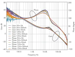
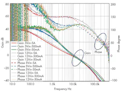
In reviewing the large-signal transient response in part 2, the input-voltage feed-forward-type VM converter has no dependency on its input voltage or output current, so completely identical Bode plots are generated from different input voltages (5 V and 12 V) and different output currents (50 mA, 500 mA and 5 A). Figure 1 shows Bode plots of all six combinations. Besides small real-world measurement variations, the six curves are identical.
Figure 1 shows that IC-VM has a phase margin around 50 deg. to 60 deg. Table 1 summarizes the exact phase-margin readings.
Output impedance
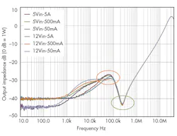
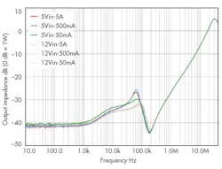
Figure 2 shows output-impedance plots of the same IC-VM. In Fig. 2, the peaks within the orange circle represent their quality factors, Q. The phase-margin numbers in column three of Table 1 are derived from these quality factors. See the appendix for details. Negative-direction peaks in the green circle are self-resonant of the output capacitor on the printed circuit board (PCB).
Small-signal load-transient response
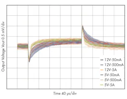
Judging from the phase-margin values in Table 1, which are all above 50 deg., ringing is not expected in a small-signal load-transient analysis. Figure 3 shows the resulting waveforms of transient analysis. In these small-signal load-transient measurements, a 20mA load-current step is applied in parallel with a DC output current of 5 A, 500 mA, and 50 mA. As expected, there is no ringing, and there are very close response waveforms in all six combinations.
1mF output capacitance
As explained in part 2, the IC-VM board does not have enough space for 1mF capacitors; the 1 mF is connected with a very short wire. In part 2, this wire appears in large-signal load transient analysis as a glitch. In all three small-signal measurements, a 1mF setting for IC-VM is not good for measuring IC performance itself, but is worth it to review the effect of parasitic components on a PCB.
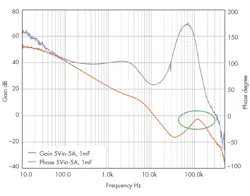
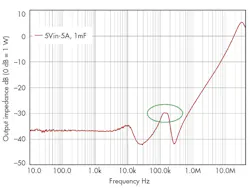
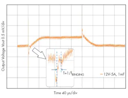
Figure 4 shows Bode plots; Fig. 5 shows output-impedance plots; Fig. 6 shows small-signal load-transient waveforms. To see clear ringing, all three results show only a 12V input and 5A output condition. By forming an anti-resonant circuit with 110µF capacitance (22 µF × 5, default capacitance) on the PCB and parasitic inductance from the 1-mF capacitor, the anti-resonant peak is introduced at around 170 kHz. This resonant peak causes:
- Second gain peak; see the green circle in Fig. 4
- Shift of the main impedance peak; see the green circle in Fig. 5
- Ringing at 170kHz frequency in Fig. 6
These figures are good examples to illustrate all three measurement methods linked as one ac-performance measurement.
CM converter
Bode plot
With the CM sample IC-CM, a bigger output capacitor gives better stability because it makes a narrower bandwidth of its control loop. Also, IC-CM2 is not stable enough just to experiment in the hopes of achieving a temporarily faster response. Here, examine IC-CM with the default 200µF operation. The loop gain of CM devices is a function of load resistance, which means it is a function of output current.
Fig. 7 shows Bode plots of all six combinations. Because a 5V input voltage is the minimum limit of IC-CM, Bode plots of 500 mA and 5 A at a 5V input start losing their bandwidth at 10 kHz and above. For an ease of observations, compare 5V input results on IC-CM; that’s why those curves are plotted in bold lines. Figure 7 also clearly shows a lower gain with a higher output current. Table 2 summarizes the exact phase-margin readings.
Output impedance
Figure 8 shows output-impedance plots of IC-CM. At around 60 kHz, these output-impedance curves at a 5V input show different peak shapes, those mean different Q factors. Table 2 also summarizes the calculated phase-margin from Q factors.
Small-signal load-transient response
Judging from the phase-margin values in Table 2, expect three to four ringing bumps at 500 mA and 5 A at a 5V input [4].
Figure 9 shows the results of small-signal load-transient analysis. As expected, the 5V input and 500mA output-current condition show multiple ringing bumps (actually, more than four bumps). As for the 5V input and 5A curve, it is difficult to see, but at least two bumps are there.
Hysteretic-mode converter
AC behavior overview of hysteretic-mode converter
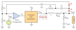
When making a Bode-plot measurement of hysteretic-mode converters, pay special attention to where to open the loop. In Fig. 10, there are two places where you could open the loop, A and B, indicated by red cross marks.
Figure 11 shows Bode plots of openings at A and B from a simple simulation model. The correct option is to open the loop at A. When choosing option B, the Bode-plot result (red lines) looks like a CM converter Bode plot because the ripple-generation circuit (Rc, Cc and Cb) is forming a local current loop.
Looking at the blue curves in Fig. 11, the LC resonant frequency is at 5 kHz where the phase turning is almost 180 deg. After the resonant frequency, the phase is recovering from 20 deg. to 60 deg. until gain crossing 0 dB at 50 kHz. This phase boost is the effect of the ripple-generation circuit and it brings stability to hysteretic-mode control.
The hysteretic-mode converter Bode plot also shows that the ripple-generation circuit is the circuit element closing an ac path for a traditional Bode-plot setup. Without the ripple-generation circuit, a hysteretic-mode converter has infinite gain, as shown in Fig. 12. By using a simple simulation model, you can plot a true open-loop gain. The gain curve in Fig. 12 shows around 80 dB of gain, which is limited by its rail-to-rail (input voltage and ground) amplitude. As this model has an LC output filter of 2 µH and 50 µF, the filter reduces the gain by 40 dB/decade from its resonant frequency of 16 kHz.
A further revelation about hysteretic-mode converters is that an unstable hysteretic-mode converter still roughly regulates its output. With VM or CM converters, an unstable loop results in a rail-to-rail oscillation from the ground to the input voltage. Unlike a VM or CM IC, a hysteretic-mode IC does not fall in a full oscillation, but shows double-pulse or multiple-pulse operation.
Figure 13 shows this triple pulse. The multiple-pulse mechanism is very simple: a hysteretic-mode converter only tries to push up its output when its feedback voltage is below its comparator threshold. So even though it is unstable, the output voltage goes high and the comparator stops pushing it up until the voltage crosses the threshold again. With a VM or CM converter, its error amplifier performs push-up and pull-down actions continuously; that is an oscillation situation.
Bode plot
The IC-HM has a pulse-skip mode. AC analysis does not offer much information at 50 mA.
Like a VM converter, response of a hysteretic-mode converter is independent from either input voltage or output current parameters. We know an output capacitor that is too large makes a hysteretic-mode IC unstable, but 1mF is still a stable region. Therefore, we do not review a 1mF case.
Figure 14 shows Bode plots of IC-HM with the default output capacitance. Using a simple simulation model confirms that the difference between 5-A and 500mA curves comes from the LC resonance (the same concept of Q factors). With a higher output current, a smaller load resistance connected in parallel with the output capacitor results in less-effective resonance. On the other hand, a smaller output current brings a higher load resistance, which results in a more ideal LC resonance. Because of the difference in resonance sharpness, phase-margin numbers are slightly different from the output-current settings.
Table 3 summarizes the exact phase-margin readings.
Output impedance
Figure 15 shows output-impedance plots of IC-HM. At 200 kHz, these output-impedance curves show their peaks. As expected from the Bode plots, these output-impedance curves are very similar in shape. Table 3 summarizes the calculated phase margins from Q factors.
By comparing Table 1 to Table 3, you’ll see there’s a distinct advantage of hysteretic-mode control, which is the loop bandwidth. A regular hysteretic-mode control has around 200 kHz to 220 kHz of bandwidth, in contrast to VM or CM’s 60kHz to 80kHz bandwidth.
Small-signal load-transient response
In Table 3, there is around 10 deg. of difference between Bode plots and output impedance because of the implementation of the ripple-injection circuit in IC-HM. In the Bode-plot measurements shown in Fig. 14, there is an ac inner loop that can’t be opened.
Based on the phase-margin values of the output-impedance curves, I expect one to two ringing bumps; from the Bode plots, I expect three to four bumps.
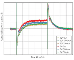
Figure 16 shows the results of small-signal load transient analysis. It is difficult to see with their noise level, but each curve shows one to two bumps. So phase-margin numbers based on output-impedance curves are a better calculation than margin numbers based on Bode plots.
Appendix
A quick summary of the relationships between output impedance and phase margin:
According to [3], Equation 1 expresses phase-margin jm value by its quality factor, Q:
A closed-loop output impedance is the open-loop output impedance divided by 1+T(s), where T(s) is the loop gain (Equation 2):
In Equation 2, the denominator is in the form of 1+T(s). The closed-loop output impedance curve (plot) graphically shows a peak expressed by its qualify factor, Q, as shown in Equation 3 and Figure A. In Equation 3, w0 is the peak frequency, w2 is the frequency of half peak in higher side, and w1 is the frequency of half peak in lower side.
Because the closed-loop output impedance is graphically measurable, Q is measurable too. Then Equation 1 gives phase margin.
References
- Steve Sandler (Picotest). How to verify control loop design. EDN, October 30, 2013.
- Steve Sandler (Picotest). Five Things Every Engineer Should Know About Bode Plots. Power Electronics, January 21, 2014.
- Robert W. Erickson and Dragan Maksimovic. Fundamentals of Power Electronics 2nd Edition. University of Colorado, 2001.
- John Stevens. Simplifying Stability Checks. Texas Instruments Application Report (SLVA381B), November 2014.
About the Author
Masashi Nogawa is a senior systems engineer for Texas Instruments’ Power Management group, where he is responsible for the SWIFT™ product line. Masashi received his bachelor’s and master’s degrees in electrical engineering from the University of Electro-Communications, Tokyo, and he holds six U.S. patents. Masashi can be reached at [email protected].
About the Author
Masashi Nogawa
Senior Systems Engineer
Voice Your Opinion!
To join the conversation, and become an exclusive member of Electronic Design, create an account today!

Leaders relevant to this article:

