Power Management 101: Power MOSFET Characteristics
What are the important power MOSFET characteristics?
To understand the planar and trench MOSFET characteristics, check several parameters critical to their performance:
- Blocking voltage (BVDSS)
- Maximum single pulse avalanche energy (EAS)
- On-resistance (RDS(ON))
- Maximum junction temperature (TJ(max))
- Continuous drain current (ID)
- Safe operating area (SOA)
- Gate charge (QG)
- Threshold Voltage (VGS(th))
- Body-Diode Forward Voltage (VSD)
- Maximum Allowable Power Dissipation (PD)
- Thermal Resistance, Junction-to-Case (Rθjc)
- dv/dt capability
- Switching and Transient Response
- ESD
The following figures are datasheet plots of the Vishay SiE848DF that is an N-channel, 30-V trench power MOSFET housed in a PolarPAK package. The MOSFET is package-limited at 60 A and 25° C.
What is the blocking voltage?
Blocking voltage, BVDSS, is the maximum voltage that can be applied to the MOSFET. When driving an inductive load, this includes the applied voltage plus any inductively induced voltage. With inductive loads, the voltage across the MOSFET can actually be twice the applied voltage.
What are the avalanche characteristics of a MOSFET?
This determines how much energy the MOSFET can withstand under avalanche conditions. Avalanche occurs if the maximum drain-to-source voltage is exceeded and current rushes through the device. The higher the avalanche value the more rugged the device. The avalanche condition can cause two possible failure modes that can destroy a MOSFET. The most destructive is "bipolar latching" that occurs if the device current causes a voltage drop across its internal device resistance, resulting in transistor action and latching of the parasitic bipolar structure of the MOSFET. A second failure mode is thermal, which occurs if the avalanche condition raises the device temperature above its maximum junction temperature.
Trench technology offers an avalanche capability approaching industry-leading planar technology. To ensure satisfactory performance, devices in this technology can be fully characterized for single pulse avalanche energy (EAS) up to their maximum junction temperature. The higher the EAS, the more rugged the device. Some devices are rated in terms of EAR, the repetitive avalanche energy.
Trench technology provides the desirable characteristics of low on-resistance sometimes at the expense of high avalanche energy. Trench power MOSFET technology provides 15% lower device on-resistance per unit area than existing benchmark planar technologies but usually at the cost of higher charge. And, the trench technology allows 10% lower on-resistance temperature coefficient.
What is power MOSFET on-resistance, RDS(on)
For both planar and trench MOSFETs, on-resistance is important because it determines the power loss and heating of the power semiconductor. The lower the on-resistance the lower the device power loss and the cooler it will operate. This is particularly important in applications where the nominal operating temperatures usually exceed 125°C. Low on-resistance drastically reduces heat-sinking requirements in many applications, which lowers parts count and assembly costs. In many applications, the low on-resistance also eliminates the need to parallel MOSFETs for low on-resistance, which leads to improved reliability and lower overall system cost than previous MOSFET generations.
RDS(on) decreases with increasing cell density. The cell density has increased over the years from around half a million per square inch in 1980 to around eight million for planar MOSFETs and around 12 million and higher for trench technology.
What are the power MOSFET temperature effects?
Whether they are planar or trench types, maximum junction temperature, TJ(max), is a function of the electrical characteristics of the device itself, as well as the package employed. Package thermal properties determine its ability to extract heat from the die. The junction-to-ambient and junction-to-case thermal resistance is a measure of the MOSFET's ability to extract heat. Datasheets rate thermal resistance in terms of either °C/W or K/W. The lower the thermal resistance, the more efficient the package is in eliminating heat. In some cases, a heat sink may be required to maintain the device junction temperature below its maximum rating. Figure 1 shows the variation of RDS(ON) with junction temperature for VGS = 4.5 V and 10 V. VGS is gate-to-source voltage.
What is the continuous drain current of a power MOSFET?
Continuous drain current, ID, establishes the ability of the MOSFET to drive a specific load. This value can be limited by the MOSFET's package. When operated in the pulsed mode, the MOSFET's drain current can be several times its continuous rating. In the pulsed mode the pulse width and duty cycle determine safe drain current and device power dissipation.
What is the SOA of a power MOSFET?
The safe operating area, SOA, for a MOSFET is a function of the voltage and current applied to the device. SOA is presented as a plot of voltage and current with the "safe" area shown in the plot. Figure 2 is the SOA plot for SiE848DF.
What is the gate charge of a power MOSFET?
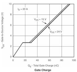
The charge on the gate terminal of the MOSFET as determined by its gate-to-source capacitance. The lower the gate charge, the easier it is to drive the MOSFET. Total gate charge, QG, affects the highest reliable switching frequency of the MOSFET. The lower the gate charge, the higher the frequency.
Operation at higher frequencies allows for use of lower value, smaller size capacitors and inductors, which can be significant factors in system cost. A low gate charge also makes it easier to drive the MOSFET, however, designers sometimes need to trade off switching frequency with EMI considerations.
Some new trench devices exhibit lower gate charge than some existing planar technologies by replacing larger die with new smaller die devices that have been optimized to offer a lower charge version of the trench devices. Figure 3 shows the gate charge for the SiE848DF, which is specified in nC, nano-coulombs.
What is the threshold voltage of a power MOSFET?
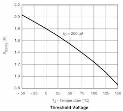
Threshold voltage, VGS(th), is the minimum gate-source electrode bias required to form a conducting channel between the source and the drain regions. It is usually measured at a drain-source current of 250 µA. A value of 2 to 4 V for high-voltage devices with thicker gate oxides, and logic-compatible values of 1 to 2 V for lower-voltage devices with thinner gate oxides, are common.
In battery-based applications where power is a premium, the trend is towards lower values of RDS(on) and VGS(th). Gate oxide quality and integrity become major issues as gate oxide thickness is reduced to achieve lower VGS(th); the minimum voltage is required between the gate and source that enables the MOSFET to turn on. Logic-level MOSFETs have typical values of about 2 V to 3 V, whereas other devices can have higher values.
In Figure 4, the threshold voltage is plotted against junction temperature. The datasheet specifies the typical threshold as 1.8 V for a drain current of 250 µA, which puts the MOSFET in the logic level range.
How do you calculate the gate current required to turn on a power MOSFET?
Although input capacitance values are useful, they do not lend themselves to calculation of the gate current required to switch the device in a given time and they do not provide accurate results when comparing the switching performance of two devices. A more useful parameter from the circuit design point of view is the total gate charge. Most manufacturers include both parameters on their data sheets.
Using gate charge, QG, the designer can calculate the amount of current required from the drive circuit to switch the device on in a desired length of time because QG = current × time. For example, a device with a gate charge of 20 nC can be turned on in 20 ms if a current of 1 mA is supplied to the gate, or it can turn on in 20 ns if the gate current is increased to 1 A. These simple calculations would not have been possible with input capacitance values.
What is the relationship between gate charge and on-resistance of a power MOSFET?
Gate charge and on-resistance are inter-related. That is, the lower the gate charge, the higher the on-resistance and vice versa. Historically, MOSFET manufacturers have focused on reducing RDS(on) without paying much attention to gate charge. This has changed in the last several years, with new designs and processes becoming available that offer reduced gate charge devices. It is important to note that there is a tradeoff between RDS(on) and gate charge and that the application will dictate which parameter is more important. The product of RDS(on) × QG is a figure of merit (FOM) that compares different power MOSFETs for use in highfrequency applications
What are the losses associated with a power MOSFET?
Because power MOSFETs are primarily used as power switches, they are expected to have low conduction and switching losses. For power management applications, conduction losses, ruggedness and avalanche capability are important features. Conduction losses are determined by the product of operating current and on-resistance (I2R) of the power MOSFET.
What is the body-diode forward voltage of a power MOSFET?
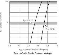
Body-diode forward voltage (VSD) is the guaranteed maximum forward drop of the body-drain diode at a specified value of source current. The value of VSD is significant and must be low in applications where the source-drain voltage may extend into the negative range, causing forward biasing the body-drain diode. If this happens, the source-drain current flows from drain straight to the source contacts, across the forward biased body-diode p-n junction.
A second and more dominant current conduction path will exist through the channel if the gate-source voltage, VGS > VGS(th). Low voltage and low RDS(on) power MOSFETs are used in such synchronous rectifier modes since their forward voltage drop can be as low as 0.1 V versus the typical Schottky diode forward voltage drops of 0.4 to 0.5 V. Maximum values of 1.6 V for high voltage devices (> 100 V) and values of 1.2 V for low voltage devices (< 100 V) are common for VSD. The source-drain diode forward voltage is shown in Figure 5 for the SiE848DF.
What is the maximum allowable power dissipation of a power MOSFET?
An important parameter is the maximum allowable power dissipation, PD, that raises the MOSFET’s die temperature to the maximum allowable junction temperature, TJ(max), when the case temperature is held at 25°C. TJ(max) is normally 150°C or 175°C.
What is the thermal impedance of a power MOSFET?
RθJC is the junction-to-case thermal impedance of the MOSFET. A typical surface-mount package can have a thermal resistance of 30 to 50°C/W, whereas a typical TO-220 device can be 2°C/W or less. Datasheets may also provide a value for RθJA for the junction-to-ambient thermal resistance of the power MOSFET.
What is the maximum dV/dt of a power MOSFET?
The maximum rate of rise of source-drain voltage allowed is the MOSFET's dV/dt. If this rate is exceeded, the voltage across the gate-source terminals may become higher than the threshold voltage of the device, forcing the device into current conducting mode and under certain conditions a catastrophic failure may occur.
There are two possible mechanisms by which a dV/dt induced turn-on may take place. One becomes active through the feedback action of the gate-drain capacitance CGD together with CGS forming a capacitive divider that can generate a pulse sufficient to exceed the Vth and turn the device on during fast voltage transitions on the drain. When a voltage ramp appears across the drain and source terminals of the device, usually the driver will sink a current flowing through the gate resistance, RG, to clamp the gate low during the off state. If RG is too large, it is sometimes possible that the driver is isolated from the gate allowing the device to turn on. RG is the total gate resistance in the circuit.
The second mechanism for the dV/dt turn-on in MOSFETs is through the parasitic BJT. The capacitance associated with the depletion region of the body diode, extending into the drift region is denoted as CDB and appears between the base of the BJT and the drain of the MOSFET. This capacitance gives rise to a current that flows through the base resistance, RB, when a voltage ramp appears across the drain-source terminals.
What affects the switching and transient response of a power MOSFET?
When the MOSFET is used as a switch, its basic function is to control drain current by a voltage signal applied to the gate. Switching performance of a device is determined by the time required to establish voltage changes across capacitances and current changes in inductances. RG is the distributed resistance of the gate and is approximately inversely proportional to active area. Values of around 20 Ω-mm2 are common for the product of RG and active area for polysilicon gates.
Figure 6 [missing - if you have a copy of the magazine or old datasheet, please send a scan to Andy] shows the parasitics in the MOSFET input. LS and LD are source and drain lead inductances and are around a few tens of nH. There are also several parasitic capacitances associated with the power MOSFET. Gate-source capacitance, CGS, is the capacitance due to the overlap of polysilicon gate with the source and the channel regions and is not a strong function of applied voltage.
How does “static electricity” (ESD) affect power MOSFETs?
Emergence of MOSFET technology has brought with it another way to kill semiconductors: static charge. The charge accumulated by a person handling an MOSFET semiconductor is often enough to destroy the part. Therefore, manufacturers of semiconductors have instituted static discharge ratings that range from 3,000 to 5,000 V. Handlers of MOSFET semiconductors use grounding straps and conductive surfaces to prevent static charge problems.
Related Power Management Articles:
- System Power Supplies
- Power Mosfets
- Converter & Controller ICs
- Application Specific ICs
- Power Management Semiconductors
- Power Peripheral and Battery-Based ICs
This updated article was originally published on May 15, 2009 in Endeavor Media's Power Electronics Technology Magazine.
About the Author
Andy Turudic
Technology Editor, Electronic Design
Andy Turudic is a Technology Editor for Electronic Design Magazine, primarily covering Analog and Mixed-Signal circuits and devices and also is Editor of ED's bi-weekly Automotive Electronics newsletter.
He holds a Bachelor's in EE from the University of Windsor (Ontario Canada) and has been involved in electronics, semiconductors, and gearhead stuff, for a bit over a half century. Andy also enjoys teaching his engineerlings at Portland Community College as a part-time professor in their EET program.
"AndyT" brings his multidisciplinary engineering experience from companies that include National Semiconductor (now Texas Instruments), Altera (Intel), Agere, Zarlink, TriQuint,(now Qorvo), SW Bell (managing a research team at Bellcore, Bell Labs and Rockwell Science Center), Bell-Northern Research, and Northern Telecom.
After hours, when he's not working on the latest invention to add to his portfolio of 16 issued US patents, or on his DARPA Challenge drone entry, he's lending advice and experience to the electric vehicle conversion community from his mountain lair in the Pacific Northwet[sic].
AndyT's engineering blog, "Nonlinearities," publishes the 1st and 3rd Tuesday of each month. Andy's OpEd may appear at other times, with fair warning given by the Vu meter pic.
Voice Your Opinion!
To join the conversation, and become an exclusive member of Electronic Design, create an account today!

Leaders relevant to this article:


