Unique MOSFETs Automatically Regulate And Balance Series-Connected Supercaps
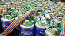
Individual supercapacitors have a 2.5 to 2.7 V maximum rating so they must be connected in series to work at higher voltages, which requires the balancing of supercap leakage currents for proper operation (Fig. 1). Now, Advanced Linear Devices (ALD) has developed Supercapacitor Auto Balancing (SAB) MOSFETs that by themselves address regulation and leakage current balancing of series-connected supercaps. Without the proper supercap balancing, overcharging could cause failure or punch through that leads to unreliable performance.
To understand how the SAB MOSFETs work, we first have to review operation of series-connected supercaps, which depends on their material and construction as well as their variable operating characteristics:
· Initial leakage current
· Initial supercap voltage
· Charging voltage
· Charging current
· Temperature range
· Aging
Therefore, problem-free operation of two or more series-connected supercaps must mitigate the impact of these variable characteristics. This requires automatic leakage current and voltage balancing of each supercap because their characteristics can vary from one supercap to another.
There have been passive approaches to voltage balancing that employ high value resistors, even though they waste power and don’t allow for aging and temperature variations. And, active balancing circuits using op amps, zener diodes, MOSFETs and resistors have also been used and they also waste power. These circuit balancing components also increase cost and board space.
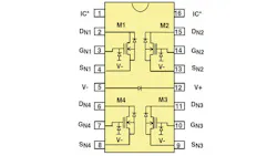
Fig. 2 shows a quad package of one these the SAB MOSFETs; there are also dual MOSFET packages. These MOSFETs have unique electrical characteristics for active continuous leakage current regulation and self-balancing of stacked series-connected supercaps. And, they dissipate near zero leakage currents, practically eliminating extra power dissipation. For most applications, automatic charge balancing with SAB MOSFETs offers a simple, economical and effective method to balance and regulate supercap voltages.
The principle behind the Supercap Auto Balancing MOSFET is basically simple. It is based on the natural threshold characteristics of a MOSFET device. The threshold voltage of a MOSFET is the voltage at which a MOSFET turns on and starts to conduct a current. The drain current of the MOSFET, at or below its threshold voltage, is an exponentially non-linear function of its gate voltage. Hence, for small changes in the MOSFET’s gate voltage, its on-current can vary greatly, by orders of magnitude. SAB MOSFETs are designed to take advantage of this fundamental device characteristic.
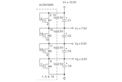
During the production process, these MOSFETs are trimmed to operate at specific threshold voltages. This produces a selection of different threshold voltages for various supercap nominal voltage values and desired leakage balancing characteristics. Each SAB MOSFET generally requires connecting its V+ pin to the most positive voltage and its V- and IC pins to the most negative voltage within the package. Each drain pin has an internal reverse biased diode to its source pin, and each gate pin has a reverse biased diode to V-. All other pins must have voltages within V+ and V- voltage limits. Fig. 3 shows a quad SAB MOSFET connected to four series-connected supercaps.
You should use standard ESD handling procedures when working with these sensitive MOSFET devices that are housed in SOIC packages. Use of these packages avoids ESD problems when trimming and also allows access to all three terminals for trimming: drain, source, and gate. If this three-terminal access wasn’t necessary, these MOSFETs could have been mounted in a two-lead package similar to that of a diode.
SAB MOSFETs provide regulation of the voltage across a supercap cell by increasing its drain current exponentially across the supercap when supercap voltages increase, and by decreasing its drain current exponentially across the supercap when supercap voltages decrease.
When a supercap in a supercap stack is charged to a voltage less than 90% of the desired voltage limit, the SAB MOSFET across the supercap turns off and there is zero leakage current contribution from the MOSFET. On the other hand, when the voltage across the supercap is over the desired voltage limit, the SAB MOSFET turns on to increase its drain currents and keep the over-voltage from rising across the supercap. Also, this simultaneously lowers the voltages and leakages of other supercaps in the stack and maintains near-zero net leakage currents.
Supercap Charging And Discharging
A supercap’s rate of charging must be limited so that excessive voltage and current do not build up across any two pins of the SAB MOSFETs, even momentarily, to exceed their absolute maximum rating (about 10 V). In most cases this is not an issue, as there may be other design constraints elsewhere in the circuit that limit the rate of charging or discharging the supercaps. For many types of applications, no further action, other than checking the voltage and current excursions, or including a simple current-limiting charging resistor, is necessary.
Consider the case when two supercap cells are connected in series, each with a SAB MOSFET connected across it in the Vt mode (VDS = VGS), charged by a power supply to a voltage equal to 2 x VS. If the top supercap has a higher internal leakage current than the bottom supercap, the voltage VS (top) across it tends to drop lower than that of the bottom supercap. The SAB MOSFET IDS(ON) across the top supercap, sensing this voltage drop, drops off rapidly. Meanwhile, the bottom supercap VS(bottom) voltage tends to rise, as VS(bottom) = (2 x VS) - VS(top). This tendency for the voltage rise also increases VGS = VDS voltage of the SAB MOSFET across the bottom supercap. This increased VGS = VDS voltage would cause the IDS(ON) of the bottom SAB MOSFET to increase rapidly as well. The excess leakage current of the top supercap would now leak across the bottom SAB MOSFET, reducing the voltage rise tendency of the lower supercap. With this self-regulating mechanism, the top supercap, VS(top), voltage tends to rise while the bottom supercap, VS(bottom), voltage tends to drop, creating simultaneously opposing actions of the supercap leakage currents.
Design Example
A single 5 V supply powers two 2.7 V supercaps connected in a series and each regulated by a SAB MOSFET.
The supercap characteristics are:
1) Maximum operating voltage = 2.70 V
2) Maximum leakage current = 10 µA at 70 °C.
3) At 2.50 V, the supercap maximum leakage current = 2.5 µA at 25 °C.
Next, pick the ALD810026 SAB MOSFET with Vt = 2.60 V. For this device, at VGS = VDS = 2.60 V, the nominal IDS(ON) = 1 µA. At VGS = VDS = 2.50 V, IDS(ON) = ~0.1 µA.
At a nominal operating voltage of 2.50 V, the additional leakage current contribution by the ALD810026 is therefore 0.1 µA. The total current for the supercap and the SAB MOSFET = 2.5µA + 0.1µA = ~2.6 µA @ 2.50 V operating voltage. At an operating voltage of 2.40 V, the additional ALD810026 leakage current decreases to about 0.01 µA.
At a maximum 2.70 V across the ALD810026 SAB MOSFET, VGS = VDS = 2.70 V results in IDS(ON) = 10 µA. 10 µA is also the maximum leakage current margin, the difference between top and bottom supercap leakage currents that can be compensated.
If a higher maximum leakage current margin is desired for an application, then go to the next SAB MOSFET down in the series, ALD810025. For an ALD810025 operating at a max. rated voltage of 2.70 V, the max. leakage current margin is ~50 µA. For this device, the nominal operating current at 2.50V is ~1µA, which is the average current consumption for the series-connected stack. The total current for the supercap and the SAB MOSFET is = 2.5 µA + 1 µA ~ 3.5 µA @ 2.50 V operating voltage.
Because the SAB MOSFET is always active and always “on”, there is no circuit switching or sleep mode involved. This may become an important factor when the time interval between the supercap discharging or recharging, and other events happening in the application, is long, unknown or variable.
In real life situations, the actual circuit behavior is a little different, further reducing overall leakage currents from both supercaps and SAB MOSFETs, due to the automatic compensation for different leakage current levels by both the supercaps themselves and in combination with the SAB MOSFETs. Take the above example of two supercaps in series, assuming that the top supercap is leaking 10 µA and the bottom one leaking 4 µA (both at the rated 2.7 V max.) while the power supply remains at 5 VDC. The actual voltage across the top supercap tends to be less than 50% of 5.0 V, due to its internal leakage current, and results in a lowered current level because the voltage across it tends to be lower as well. The total voltage across both supercaps is still 5.0 V, so each supercap would experience a lowered voltage at less than maximum rated voltage of 2.7 V, thereby resulting in reduced overall leakage currents in each of the two supercaps.
These leakage currents are then further regulated by the SAB MOSFETs connected across each of the supercaps. The end result is a compensated condition where the top supercap has ~2.4 V and the bottom cap has a voltage of ~2.6 V. The excess leakage current of the top supercap is bypassed across the bottom SAB MOSFET, so that there is little or no net additional leakage current introduced by the bottom SAB MOSFET. Meanwhile the top SAB MOSFET, with ~2.4 V across it, is biased to conduct (or leak) very little drain current. Note also that the top supercap is now biased at ~2.4 V and, therefore, would experience less current leakage than when it is at 2.7 V. The primary benefit here is that this process of leakage balancing is fully automatic and works for a variety of supercaps, each with a different leakage characteristic profile of its own.
A second benefit is that with ~2.4 V and ~2.6 V across the two supercaps, in this example, the actual current level difference between the top and the bottom SAB MOSFETs is at about a 100:1 ratio (~2 orders of magnitude). The net additional leakage current contributed by the ALD8110026 in the design example above would, therefore, be approximately 0.01 µA. In this case, the difference in leakage currents between the two supercaps can have a ratio of 100:1 and could still have charge balancing and voltage regulation.
The dynamic response of an SAB MOSFET circuit is very fast, and the typical response time is determined by the R C time constant of the equivalent ON resistance value of the SAB MOSFET and the capacitance value of the supercap. In many cases the R value is small initially, responding rapidly to a large voltage transient by having a smaller R C time constant. As the voltages settle down, the equivalent R increases. As these R and C values can become very large, it can take a long time for the voltages across the supercaps to settle down to steady state leakage current levels.
About the Author

Sam Davis
Sam Davis was the editor-in-chief of Power Electronics Technology magazine and website that is now part of Electronic Design. He has 18 years experience in electronic engineering design and management, six years in public relations and 25 years as a trade press editor. He holds a BSEE from Case-Western Reserve University, and did graduate work at the same school and UCLA. Sam was the editor for PCIM, the predecessor to Power Electronics Technology, from 1984 to 2004. His engineering experience includes circuit and system design for Litton Systems, Bunker-Ramo, Rocketdyne, and Clevite Corporation.. Design tasks included analog circuits, display systems, power supplies, underwater ordnance systems, and test systems. He also served as a program manager for a Litton Systems Navy program.
Sam is the author of Computer Data Displays, a book published by Prentice-Hall in the U.S. and Japan in 1969. He is also a recipient of the Jesse Neal Award for trade press editorial excellence, and has one patent for naval ship construction that simplifies electronic system integration.
You can also check out his Power Electronics blog.
Voice Your Opinion!
To join the conversation, and become an exclusive member of Electronic Design, create an account today!

Leaders relevant to this article:


