Moving on to GaN Switches in Switch-Mode Power Supplies
What you'll learn:
- What challenges emerge when replacing silicon MOSFETs with GaN devices?
- Steps to building a GaN-based design.
- Simplifying the design process with a GaN controller.
A common question comes up among power-management design engineers these days: “Is it time to switch from silicon power switches to GaN-based ones? Gallium-nitride (GaN) technology offers many advantages over traditional silicon-based MOSFETs. As a wide-bandgap semiconductor, GaN allows power switches to operate at high temperatures and achieve high power density.
Due to its high breakdown voltage, GaN is suitable for applications above 100 V. Even below 100 V, its high power density and fast switching capability provide benefits like higher power-conversion efficiency in various power-supply designs.
The Challenges When Using GaN Devices
No doubt, some challenges will arise when replacing silicon-based MOSFETs with GaN devices. First, GaN switches typically have lower gate-voltage ratings. Hence, it’s important to ensure that driver stages are strict in limiting the maximum voltage to avoid damage to the GaN device.
Then one must deal with the fast voltage change (dv/dt) of the power supply’s switch node. This may cause false turn-on of the bottom switch. To solve this problem, a separate pull-up and pull-down pin and a carefully designed printed-circuit-board (PCB) layout are needed.
>>Download the PDF of this article. Also, check out these TechXchanges for similar articles and videos
Lastly, GaN FETs have a higher conduction loss during dead times. One way to solve this problem is to strictly minimize dead times. This needs to be done without generating overlapping times of the high- and low-side switches to avoid a short circuit to ground.
How to Get Started with a GaN Design
With the alluring promises of GaN in power-supply design, a basic question is how to get started. A simple way is to select a switch-mode power-supply (SMPS) controller IC, such as Analog Devices’ (ADI) LTC7891 single phase, step-down (buck) GaN controller. Selecting a dedicated GaN controller makes a GaN power-supply design simple and robust.
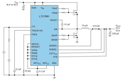
All of the challenges previously mentioned are addressed and solved with such controllers. Figure 1 shows the simplicity of a step-down power design using GaN FETs controlled by a dedicated GaN controller like the LTC7891.
If an existing power supply with an existing controller IC needs to be repurposed to control a GaN-based power supply, it makes sense to use a dedicated GaN driver. It takes care of solving the challenges with GaN and allows for a simple and robust design. Figure 2 shows the power stage of a buck regulator implemented with an LT8418 driver IC.
Taking the First Steps
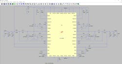
Once suitable hardware, controller IC, and GaN switches have been selected, a great way to get the first evaluation results is via a detailed circuit simulation. ADI’s LTspice offers complete circuit models that may be used for simulation free of charge. It provides a convenient way to learn about using GaN switches. Figure 3 shows a simulation schematic with the LTC7890, a dual-channel version of the LTC7891.
Making the Move to GaN
GaN technology for switch-mode power supplies has reached a solid development state in which many power-supply applications can be designed with them. However, each new generation of GaN switches will undergo further development. The existing SMPS controllers and drivers for GaN from ADI are a flexible, yet dependable way to work with GaN FETs from different vendors now and in the future.


