Power-Supply Subsystems for PPG Remote-Patient Vital Sign Monitors (Part 1)
This article is part of TechXchange: Power Supply Design series: Power-Supply Subsystems for Remote PPG Vital Sign Monitors
Members can download this article in PDF format.
What you’ll learn:
- Learn how to select a power-supply configuration based on PPG system requirements.
- Review the implementation of switched-mode power-supply reference circuits for both discrete (part one) and integrated designs (part two).
- A power-supply performance test methodology that validates the system over different device use cases and transient loading conditions.
- Get a checklist to validate the implementation.
- Gain troubleshooting knowledge to address implementation issues.
A photoplethysmogram (PPG) device can be implemented to measure blood volume changes from which vital sign information such as blood oxygen levels and heart rates are derived. In Part 1, we provide discrete power-supply circuit design solutions for best performance using the MAX86171 optical pulse oximeter and heart-rate sensor analog front end (AFE). Part 2 examines an integrated solution for space-constrained applications.
Switch-mode power supplies (SMPS, also referred to as dc-dc converters) are commonly used in wearable medical and healthcare applications for reasons such as size considerations and power efficiency. Designers can use these power supplies to create battery-operated products that achieve longer lifetimes. Unfortunately, designers are still left to select the appropriate SMPS device followed by creating a suitable circuit board layout that preserves the performance of a biosensing device in their system.
To help simplify and speed the process, Analog Devices developed power-supply subsystem circuit designs that have been pre-validated (i.e., designed, built, and tested) to ensure the signal-to-noise ratio (SNR) performance of each biosensing AFE device. This article provides details for the power-supply circuits, with each example being complemented with a validation checklist and troubleshooting guide to aid circuit designers, if needed.
Figure 1 shows a standard power block diagram encountered in many remote-patient monitoring applications. Table 1 reveals the design limits, and Table 2 shows the design considerations for discrete and integrated solutions.
Discrete Design Description
This DC-DC converter design regulates the three-output power supply rails for use in a remote patient vital sign monitor subsystem. The circuit provides proper line and load regulation while maintaining low output noise levels to preserve biosensing SNR performance, which is powered by a rechargeable lithium polymer battery or a primary Li Cell battery.
Figure 2 shows the PPG subsystem using discrete power supply devices and Table 3 lists the main components.
1.8-V SMPS Circuit Using a nanoPower Buck Converter
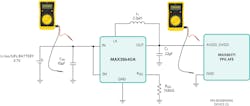
The following circuit based on the MAX38640A nanoPower buck converter (Fig. 3) shows the typical input and output power-supply level to properly operate the SMPS device in remote-patient vital sign monitor applications.
As illustrated in Figure 3, a digital multimeter (DMM) can be used to probe the input and output ports to validate the supply voltage levels. The power-supply output levels can vary due to various factors such as a discharging battery or changing loads (i.e., device mode changes, devices waking up from sleep mode, etc.).
1.8-V SMPS Circuit Validation Checklist
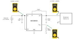
The circuit validation checklist (Table 4) is intended to help designers with their electrical bench checkout of the 1.8-V SMPS circuit post board assembly (Fig. 4). In this case, the MAX38640A device, while connected to a biosensing circuit load, is used This checklist also can be employed as a template for product testing.
Troubleshooting the MAX38640A (1.8-V Output) SMPS Circuit
These circuit troubleshooting instructions will help designers if operational issues arise with the operation of the 1.8-V SMPS circuit (Fig. 5). This guide addresses the most common problems that crop up when implementing these switch-mode power supplies.
Step 1: Check the input voltage
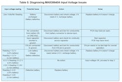
Using a DMM with an internal impedance of 1 MΩ or larger (e.g., Fluke 87), measure the voltage across at the input to the MAX38640A device. Be sure to connect the negative “black” lead to the ground and the positive “red” lead to the input “IN” pin of the device. If the input pin isn’t easily accessible, place the leads across the input capacitor (CIN). Use Table 5 to diagnose and fix associated problems.
Step 2: Check the inductor signal waveform
Using an oscilloscope or digital storage scope (DSO), probe the LX pin on the MAX38640A device. If the input pin isn’t easily accessible, place the probe on the inductor end capacitor. Note: It’s recommended that the oscilloscope and probes used have a minimum bandwidth of 200 MHz.
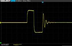
If the circuit is operating with a light load (i.e., less than 50 mA), the waveform should appear as shown in Figure 6.
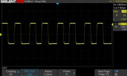
If the circuit is operating with a heavy load, the waveform should be a square wave with minimal ringing on the rise and falling edges (Fig. 7).
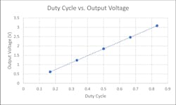
The square-wave amplitude should be approximately equal to the input battery voltage. The square-wave floor voltage should be about 200 to 300 mV below ground (e.g., −250 mV). The duty cycle is proportional to the output voltage. Thus, a 3.6-V input battery voltage will have an approximately 50% duty cycle when producing an output voltage of 1.8 V. Figure 8 shows the relationship between the duty cycle and the output voltage.
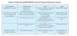
Deviations from the ideal square wave can be used to effectively diagnose and fix many problems (Table 6).
Step 3A: Check the output dc voltage
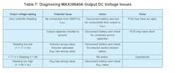
Using a DMM with an internal impedance of 1 MΩ or larger (e.g., Fluke 87), measure the voltage at the output of the MAX38640A device. Be sure to connect the negative “black” lead to the ground and the positive “red” lead to the output “OUT” pin of the device. If the output pin isn’t easily accessible, place the leads across the output capacitor (COUT).
Use Table 7 to diagnose and fix associated problems.
Step 3B: Check the output ac voltage
Using an oscilloscope or DSO, now measure the output ripple (ac) by probing the OUT pin on the MAX38640A device. To properly measure the output and minimize RF pickup, it’s recommended that 10x pigtail probes be used. Differential active probes also can be employed to further reduce ambient noise. Note: It’s recommended that the oscilloscope and probes have a minimum bandwidth of 200 MHz.
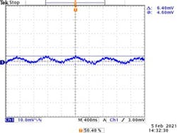
If the circuit is operating correctly, the waveform should be a 1.8-V dc output with a small ripple waveform superimposed on it. Figure 9 shows the ripple waveform.
Use Table 8 to diagnose and fix associated problems.
5.0-V SMPS Circuit Using a Low-Noise Buck-Boost Converter
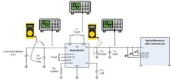
The following circuit based on the MAX20343H low-noise buck-boost converter shows the typical input and output power-supply levels for a properly operating SMPS device in remote-patient vital sign monitor applications.
A DMM can be used to probe the input and output ports to validate the supply voltage levels (Fig. 10). The power-supply output levels can vary due to various factors such as a discharging battery and changing loads (i.e., device mode changes, devices waking up from sleep mode, etc.).
5.0-V SMPS Circuit Validation Checklist
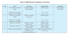
The following circuit validation checklist (Table 9) is intended to help designers with their electrical bench checkout of the 5.0-V SMPS post circuit board assembly. In this case, the MAX20343H device, connected to a biosensing circuit load, is used. This checklist also be applied as a template for product testing.
Troubleshooting the MAX20343H SMPS Circuit
These circuit troubleshooting instructions (Fig. 11) will help designers if operational issues arise with operation of the 5.0-V SMPS circuit. It addresses the most common problems that arise in implementing these switch-mode power supplies.
Step 1: Check the input voltage
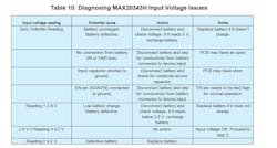
Using a DMM with an internal impedance of 1 MΩ or larger (e.g., Fluke 87), measure the voltage across the input to the MAX20343H device. Be sure to connect the negative “black” lead to the ground and the positive “red” lead to the input “IN” pin of the device. If the input pin isn’t easily accessible, place the leads across the input capacitor (CIN).
Use Table 10 to diagnose and fix associated problems.
Step 2: Check the inductor signal waveform
Using an oscilloscope or DSO, probe the HVLX pin on the MAX20343H device. If the input pin isn’t easily accessible, place the probe on the inductor end cap. Note: It’s recommended that the oscilloscope and probes have a minimum bandwidth of 200 MHz.
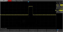
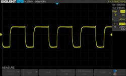
If the circuit is operating correctly, the waveform should be a pulse wave with minimal ringing on the rise and falling edges (Fig. 12).
The 500-ns pulse-wave amplitude should be approximately equal to the input battery voltage. The pulse-wave floor voltage should be within 100 mV of the ground. The output frequency and duty cycle of the pulse wave are proportional to the load current. Figures 13 and 14 show the output wave and signal frequency under different load conditions.
Deviations from the ideal square wave can be used to effectively diagnose and fix many problems. Use Table 11 to diagnose and fix associated problems.
Step 3A: Check the output dc voltage
Using a DMM with internal impedance of 1 MΩ or larger (e.g., Fluke 87), measure the voltage at the output of the MAX20343H device. Be sure to connect the negative “black” lead to ground and the positive “red” lead to the output “OUT” pin of the device. If the output pin isn’t easily accessible, place the leads across the output capacitor (COUT).
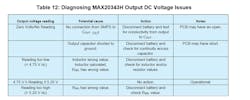
Follow the guidelines in Table 12 to diagnose and fix associated problems.
Step 3B: Check the output ac voltage
Using an oscilloscope or DSO, now measure the output ripple (ac) by probing the OUT pin on the MAX20343H device. To properly measure the output and minimize RF pickup, it’s recommended that 10x pigtail probes be used. Differential active probes also can be utilized to further reduce ambient noise. Note: It’s recommended that the oscilloscope and probes have a minimum bandwidth of 200 MHz.
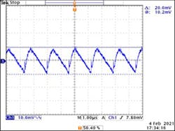
If the circuit is operating correctly, the waveform should be a 1.8-V dc output with a small ripple waveform superimposed on it. Figure 15 shows the ripple waveform.
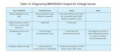
Table 13 can be used to diagnose and fix associated problems.
Conclusion
Pre-validated discrete power supply circuits were presented in this article that can be used with the MAX86171-based PPG remote patient vital sign monitor. These power-supply circuits will work with MAX86141-based PPG devices as well.
In Part 2, we present pre-validated integrated power-supply circuits for use with both MAX86171- and MAX86141-based PPG remote-patient vital sign monitors.
The corresponding validation test data for both discrete and integrated power-supply implementations can be found on the Maxim Integrated, now part of Analog Devices, website at “Power Supply Subsystems for Remote Patient Vital Sign Monitors.”
References


