Does a DC-DC Converter Have to be Synchronous for Low Emissions?
Members can download this article in PDF format.
What you'll learn:
- How nonsynchronous converters can offer low emissions by implementing catch diodes.
- Layout considerations for nonsynchronous converters.
- The highly beneficial aspect of controlled switching.
Synchronous Silent Switcher converters have set the standard for powerful, compact, and quiet dc-dc conversion. We’ve been introduced to a plethora of these low-electromagnetic-interference (EMI) synchronous buck and boost converters in the past 5+ years.
Such dc-dc converters have simplified the system-level electromagnetic-compatibility (EMC) design in high-power, noise-sensitive environments such as cold-crank preboosts, driving high-current LED strings, and high-voltage power-amplifier sound systems. Monolithic (integrated power switch) boost regulators provide an efficient and more compact solution compared to a controller-based design and are commonly used from source voltages of 5, 12, and 24 V.
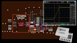
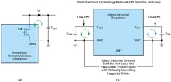
Integrated synchronous switches and their unique layout within the silicon1 are part of the secret sauce of Silent Switcher converters (Fig. 1). On-board (integrated) switches create super-tiny hot loops, which help keep emissions at a bare minimum. However, this can come with a cost, and synchronous switches may not be necessary in all applications.
Switching converters can be lower cost if only a single power switch is integrated into the silicon, and we can rely on an external, low-cost, discrete catch diode to act as the second switch. This is common practice for lower-cost converters, but is this okay to do when low emissions are important?
Nonsynchronous converters with discrete catch diodes can still achieve low emissions. It’s possible to design low-EMI switching applications with nonsynchronous converters by paying special attention to both the hot-loop layout and the dV/dt switching edge rate (Fig. 1, again).
Incorporating additional emission reduction with spread-spectrum frequency modulation (SSFM) is a must. Monolithic switching regulators such as the LT3950 60-V, 1.5-A nonsynchronous LED driver and the LT8334 40-V, 5-A nonsynchronous boost converter each have a single, low-side power switch integrated into their devices. However, they rely on external catch diodes while still achieving low emissions! How does this work?
Catch Diodes vs. Dead Time
Integrating a single power switch vs. two in a monolithic converter can reduce die size by 30% to 40%. Die-size reduction has direct silicon cost savings and an additional, secondary cost savings when the silicon can fit into a smaller package. Although some PCB space still needs to be dedicated to an external, discrete catch diode, these diodes are plentiful, robust, and cheap. In a boost converter, the Schottky diodes with low VF perform with high efficiency at high output voltage and low duty cycle—arguably outperforming expensive high voltage power FETs.
One reason might be due to dead time. In typical synchronous converters, power-switch body-diode conduction occurs during a preset dead time to prevent potential shoot-through disasters. Shoot-through occurs when the synchronous switch turns on before the main switch can completely turn off—creating a direct short to GND from the input or output (buck or boost).
Dead-time control can be a limiting aspect of switcher design at high switching frequency and minimum and maximum duty-cycle limits. Low-cost catch diodes with low forward voltage eliminate the need for dead-time logic in a switcher—simple. In most cases, they also outperform the forward voltage drop of the inherent body diodes inside the power switches (which do conduct during dead time).
Simple Layouts and Packages
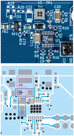
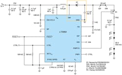
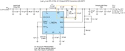
First, we can start with a simple monolithic boost converter to demonstrate a basic layout. The LT3950 LED driver in Figure 2 has a simple PCB hot loop. This hot loop, highlighted in Figure 3, only includes the small, ceramic output capacitor and the discrete catch diode of similar size, PMEG6010CEH. These components fit snuggly with the LT3950 16-lead MSE package and the switching pins and GND plane of the thermal pad.
Is this enough for low emissions? It sure is part of the equation. The wire-bonded, 16-lead MSE package and tight hot loop can achieve low emissions when combined with SSFM and well-controlled switching behavior (switching edge transitions that don’t ring due to very high speed and parasitic trace inductance).
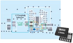
Next, the single switch of a nonsynchronous converter can be used to create a SEPIC topology (step-up and step-down), extending the usefulness beyond just the intended boost designation. The single switch makes it easy to break the hot loop of the boost and add the SEPIC coupling capacitor shown in Figures 4 and 5.
Most synchronous boost converters whose top and bottom switches are connected permanently at a single switch node can’t be converted into a SEPIC. The SEPIC hot loop can remain small if attention is paid to the loop formed by the coupling capacitor, the catch diode, and the output capacitor.
The LT8334 nonsynchronous boost converter has an integrated 5-A, 40-V switch. This monolithic step-up converter IC is useful for making 12-V output SEPIC converters.
Figure 4 shows a standard 12-V, 2-A+ SEPIC converter with coupling capacitor C1 and two inductive windings of a coupled inductor. Since the tiny PMEG4030ER catch diode (D1) isn’t affixed directly to the switching node, the 4.7-μF 0805 ceramic, dc-blocking, coupling capacitor can be placed between the diode and the switching node with ease. The hot-loop layout remains small on the EVAL-LT8334-AZ SEPIC evaluation board.
Keeping the switching-node copper as small as possible and as close to the switching pin as possible helps minimize radiated emissions. Please note that the entire hot loop is placed on Layer 1 and there are no vias on either the switching node or the coupled switching node on the other side of the coupling capacitor. Both switching nodes should be kept to minimum size and as close as possible for the best results. The 12-lead DFN package of the LT8334 helps keep the hot loop and emissions as small as possible.
Controlled Switching Is Effective
Monolithic (switch-included) switching converters are quite effective at emission reduction when combined with SSFM, 2-MHz fundamental switching frequency, excellent PCB layout, and well-controlled switching. If they’re effective enough, they may not need the extreme benefits of Silent Switcher architecture for low emissions (the Silent Switcher is recognized as the top architecture for ultra-low emissions, but not necessary in all circumstances just to pass emission standards).
In the LT3950 and LT8334, SSFM spreads from the fundamental frequency to about 20% higher and back in a triangle pattern. SSFM is a common feature among low-EMI switching regulators.
There are a variety of SSFM types, but the overall goal of each is to spread out the emission energy and reduce the highest points of peak and average emissions below the required limits. One goal of 2-MHz switching frequency is to set the fundamental switching frequency above the AM radio band (530 kHz to 1.8 MHz) limit. Therefore, the fundamental itself and all of its harmonics create emissions without disturbing the radio. When there’s no concern for the AM band, a lower switching frequency can be used.
Independent of switching frequency, the internal switch and driver should be designed carefully to avoid certain unwanted behaviors that deteriorate EMI performance in switching converters. Ultra-fast, ringing switch waveforms can cause unwanted emissions in the 100- to 400-MHz range, which can be most noticeable on radiated emission measurements.
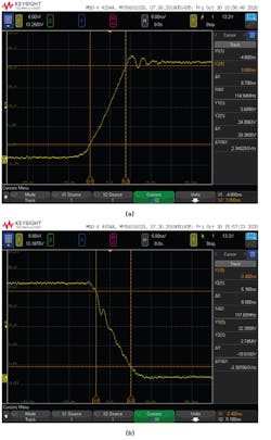
A well-controlled switch inside the IC should act less like an emission hammer and more like an effective rubber mallet with its switching edges dampened. A controlled power switch moves high voltage and current up and down at a slightly reduced rate below what’s possible.
The 2-V/ns switch rate and lack of ringing in Figure 6b is a great example of this controlled switching in a monolithic converter. You can see how soft this internal switching turns on and lands gently at 0 V, without a harsh ring beyond. This is a major contributor to the emission results of the LT3950 (see figures 9 to 11 below). Normally, in a monolithic switching regulator, the speed of the switch drives up the maximum power and reduces the thermal dissipation. However, when carefully designed, less can be more.
Nonsynchronous Boost Controller with Gate Rate Control
At some point, high power dc-dc conversion requires a controller and high-voltage, high-current switches external to the IC. In this case, the gate driver for an external switch remains inside the IC, but the entire switching hot loop moves outside of the IC. Some creative hot loops and layout are possible, but the hot loop itself typically grows due to the size of the discrete MOSFET(s) alone.
In one example, the LT8357 high-power (nonsynchronous) boost controller provides 24 V, 2 A (48 W) with very low emissions. It powers a 3.5- × 3.5-mm MOSFET at a low switching frequency for efficient conversion. In addition to the tight hot loop (Fig. 7), it also has rising and falling gate control pins for edge-rate control and emission reduction.
A simple 5.1-Ω resistor RP (on GATEP) is enough to reduce the turn-on edge rate of the M1 power MOSFET and keep radiated emissions at a minimum. Of course, some emission filters and SSFM help with emission reduction. An additional place for an emission shield is provided for the EVAL-LT8357-AZ evaluation board, but it might not be necessary for most applications.
Thus, this nonsynchronous boost controller, much like its monolithic counterparts, has all of the features necessary for high-power, low-EMI boost, and SEPIC applications (Fig. 8).
Passing CISPR 25 Class 5 Emissions
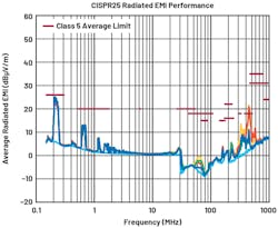
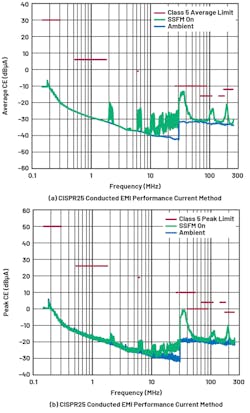
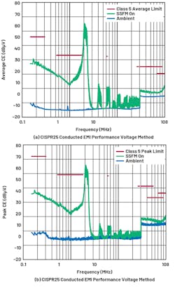
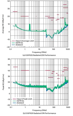
Low-EMI evaluation circuits like the LT3950 DC2788A have been tested extensively for radiated and conducted emissions. The emission test results shown in Figures 9 to 11 were captured with SSFM turned on, 12-V input, and 330-mA current through a 25-V LED string. Both current-probe and voltage-method CE results passed the most stringent limits. It’s common to have FM band CE challenges in switchers, but the LT3950 coasted by the FM band.
Setting the switching frequency to 2 MHz (300-kHz to 2-MHz adjustable range) allows the fundamental switching emissions to remain above the AM radio band (530 kHz to 1.8 MHz) and out of trouble while eliminating the need for a bulky LC AM band filter on the front end. Instead, the EMI filters used by the LT3950 can be small, high-frequency ferrite beads.
The LT8334 SEPIC also has low emissions despite the additional coupling capacitor in the hot loop and the extra terminals of the coupled inductor (which doubles the number of switching nodes). In addition, using 2 MHz and SSFM, the EVAL-LT8334-AZ SEPIC 12 VOUT evaluation kit has low emissions. The EVAL-LT8357-AZ boost controller can achieve similar performance.
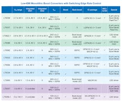
ADI’s latest family of low-EMI nonsynchronous boost and SEPIC converters is listed in the table. Monolithic and controller ICs are useful for their simple construction, low cost, multiple topologies, high power capability, and low emissions. High-current Silent Switcher boost converters also are available when ultra-low emissions are needed above all else.
Conclusion
Both synchronous Silent Switcher and nonsynchronous monolithic switching regulators can be used in low-emission applications. Nonsynchronous boost converters are lower cost when compared to the high-performance Silent Switcher converters. The second switch is replaced by low-cost catch diode, which has some advantages at high voltage and adds flexibility when reconfigured as a SEPIC.
Small plastic packages and well-designed, small hot switching loop areas of the PCB have low emissions when the power switch edge rate is well controlled with limited ringing. These features should be combined with other low-EMI features such as SSFM and EMI filters. Even in high-power boost controllers, gate-drive control is useful to slow down and smooth out the switching edges for low emissions. Pay special attention to the best possible top-layer layout of the hot loop and choose your dc-dc converters wisely for low-emission designs.
Reference
1. Steve Knoth. “High Power Density in a Small Form Factor.” Analog Dialogue, Vo. 53, No. 4, October 2019.
