In electronic systems, wires and cables provide intentional circuit paths for power or signal currents to move from a source to a load and then return to the source. These current paths have the topology of a loop.
It is easy to visualize a loop as an energy transducer in a system containing an RF source and load. And, loops are everywhere. Some are big; some are small. They appear within chips where little hair-like traces interconnect millions of transistors, on PCBs and backplanes where the trace loops are larger but fewer, within equipment modules and subsystems, and especially in interconnect cables where loop areas can be extremely large.
Sometimes the loop is so poorly defined or obscure that it is difficult to comprehend there really is a loop and that it is returning current to a source. This is especially true with wires and cables because they appear single ended.
If the circuits being driven do not have a stable, well-defined return path, the current will return to its source the best way it can, which unfortunately may be the worst way for EMC. These strange return paths generally are unacceptable. They increase radiated emissions from the circuit, capacitive and inductive cross-coupling or crosstalk between circuits, and the susceptibility of circuits that are closely coupled to the undefined path�most of the time by wires and cables.
That�s the reason for the emphasis on controlling the wiring design. Controlling the circuit loop area probably is the most important element in meeting EMC requirements. As the loop area increases, the levels of generated or intercepted energy will increase.
Loop Area
Unfortunately, since wiring and cable placement is the principle determinant of loop area, there is a limit on how small the radiated emissions or susceptibility loop can be because of physical constraints imposed by the components that comprise the system. The loop cannot be smaller than the area required by component placement. Even then, for physically large systems with high operating frequencies, this may not result in a loop area small enough to meet the requirements.
Consider as an example a system that requires several large cabinets of equipment located on two different floors or in two different buildings. Consequently, layout alone cannot be expected to completely solve the emissions or susceptibility problems.
Accordingly, other suppression techniques must be used to meet these EMC requirements. These techniques must rely on reducing signal current and limiting both bandwidth and amplitude. However, keeping loop areas as small as possible, especially for the high-frequency signals, is the most important design requirement.
The loop can be driven by the source or terminated by the receptor, which will determine whether the problem is one of emissions or susceptibility. If the loop leaves the confines of the system, the unwanted RF current in the wire or cable loop forms an internal culprit source and represents a conducted emissions problem. If the cable loop is directly connected to an external source of unwanted RF current, then there is a potential conducted susceptibility problem.
Although the wire and cable series inductance and shunt capacitance create a low-pass filter, unless the cable is really long or the frequencies are really high (at which point standing waves will occur creating yet another problem), the bandwidth generally is large enough to accommodate the RF energy. Since the various wires in the cable are closely coupled over the entire length, this results in high-level crosstalk within the cable, which increases with both amplitude and frequency.
In addition, cable loops make good antennas that unfortunately work well for both radiated emissions and radiated susceptibility coupling, especially in the near field. Handling the radiated coupling to and from the loop generally is a more difficult EMC challenge than handling the conducted coupling problem.
Differential Mode and Common Mode
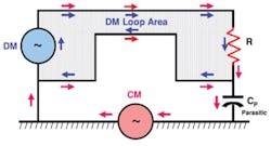
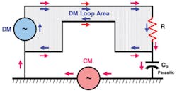
Unless the circuit loop is completely isolated from all other conductive surfaces, each loop will have two coupling modes: the differential mode (DM) and the common mode (CM). The DM, typically a differential pair over a ground plane in a high-speed system, and CM, where some synchronous current from both the signal and its associated return lead is conducted via a common reference surface, are illustrated in Figure 1.
Figure 1. CM and DM Mode Current Loops
High-level DM currents generally are the intended signals and travel from the source to the load over wire pairs such as the signal lead and the associated return lead. These DM currents are equal but travel in opposite directions.
DM is called normal mode by telecommunications designers, a description that provides better visualization and understanding. Since the signal current and the return current are traveling in opposite directions, if the conductors had coaxial alignment, cancellation would occur. This can�t happen because they are separated by a small distance equal to 2x the insulation thickness. This forms a single large loop with an area equal to the length of the cable multiplied by 2x the insulation thickness.
Still, as long as the two conductors are close together, the loop area will be smaller, much of the field will be cancelled, and the radiation will be reduced. It�s a good thing that happens; otherwise, every intentional signal in every electronic box would be a significant radiator.
The reverse is true as well. An external radiated RF source can couple into this loop and induce an unwanted differential current that may interfere with the intentional DM signal.
Two additional techniques can be used to further reduce the DM coupling. The first is twisting the wire pairs together. This replaces the large single loop with a series of smaller loops where each adjacent loop is 180 degrees out of phase with its neighbor, providing further field cancellation.
The second is cable shielding. Since the cable shield completely encloses the DM loop area, it can be used to reduce the radiation or susceptibility of the DM loop. The principal limiting factors will be the quality of the shield and the connectors.
Electric Field Produced by DM and CM Currents
The electric field (EF) radiation created by DM current circulating around a small, nonresonant loop oriented at angle (
?) is given by Kraus as:
By orienting the loop for maximum emissions, something that is done during the EMC measurements by rotating the unit, raising and lowering the antenna, and changing the antenna polarization angle, sin (?)
= 1. Converting to frequency instead of wavelength, F(MHz) � ? (m) = 300 m/�s, and introducing the attenuation provided by shielding, S, the equation can be rewritten as:
where: ? (max) = �V/meter
A = radiating loop area (sq cm), 0.1<(l/w)<10
I = drive current (amps)
F = emissions frequency (MHz)
r = measurement distance (meters)
S = shielding effectiveness ratio
Kraus indicates that for frequencies below resonance it is accurate to within 1% for loops up to 10 x 10 inches. This makes it ideal for PCB design.
However, it certainly is usable for any loop current at frequencies below loop resonance where the length to width ratio is ?10. As the loop width or wire spacing becomes smaller and smaller as in the case of a cable, the loop analysis fails. A 2-meter cable length generally is taken as the upper limit for loop analysis of cables.
A similar equation could be developed for RF pickup into the loop, but the solutions to both the emissions and susceptibility problems are nearly identical.
All conductors have series inductance (L) and are coupled to the underlying ground plane or other closely coupled conductors via unbalanced parasitic shunt capacitance (CP). These conductor characteristics unbalance the signal and its return, create the CM loop, and result in differential signal skew. Consequently, small CM currents, called longitudinal mode by telecommunications designers, arise from the unbalanced LC characteristics of the signal and associated signal return leads with respect to any closely coupled underlying return path, usually the chassis or grounding system.
These CM currents travel simultaneously in the same direction on each signal and return conductor and can be visualized as returning via a capacitively coupled return path in the nearby conducting surfaces. At the lower frequencies, this forms an antenna structure very similar to a monopole antenna oriented parallel to the cable runs.
At the higher frequencies where the cable lengths are a wavelength or longer, the structure becomes a traveling-wave antenna. In both of these antenna structures, the loop current is returned via the ground reference.
For an electrically short monopole antenna of length l, the electric field ? (?) radiation created by the CM current on the cable can be approximated by:
By orienting the antenna for maximum emissions, sin (?) = 1 and the equation can be rewritten as:
where: ? (max) = �V/meter
l = cable length in meters
I = drive current (amps)
F = emissions frequency (Hz)
r = measurement distance (meters)
The CM-generated EMI levels predicted from this antenna model correspond well with measured data.
Antenna Capture Areas
While on the subject of antennas, all conductors can be antennas. Good conductors work best, but even poor conductors can be poor antennas. And that may be all it takes for a product to fail its EMC qualification test.
The amount of RF energy collected by or radiated from an antenna is related to its capture area. From the measured RF energy, the equivalent antenna cross-sectional area can be determined. For example, a simple resonant ?
/2 dipole, terminated into a matched load impedance, has an effective cross-sectional area of 0.13 ?2. This area can be approximated by a ?/2 x ?/4 rectangle, ?2/8, or by an ellipse with major axis diameter of ?/2 and minor axis diameter of approximately ?/3. A ?/2 dipole will reradiate or scatter an amount of RF energy equal to what it absorbs.
For a nonresonant electrically short wire of length l (where l?/2), terminated in a matched load, the effective cross-sectional area is approximately 0.119 ?2. Because the load is matched, this conductor will reradiate an amount of RF energy equal to what it absorbs. Keep in mind that the energy collected is related to the effective cross-sectional area. The larger the area, the greater the RF energy collected regardless of whether the antenna is resonant.If a dipole antenna is not connected to a matched load, the ratio of absorbed to scattered energy changes. For example, if a short is placed across the leads of a ?
/2 dipole, no power can be delivered to the load, but the antenna still collects radiated RF energy. In this case, the effective cross-sectional area is 0.52 ?2, and the dipole will reradiate all of this power.
The energy level will peak when the wire is resonant and be substantially less off resonance. The reradiated RF energy from the shorted dipole is 4.37x greater than that from the terminated dipole.
Considering that a shorted dipole is simply an isolated conductor of length ?/2 located in space, this means that an unused wire in a cable or an isolated conducting surface within a cabinet or on a PCB must be removed, tied to the ground reference, or terminated in some fashion. If that is not done, it will collect and reradiate large amounts of RF energy, especially at resonance.
For example, one printer manufacturer has a plotter with a large chunk of ferrite around its stainless steel pen support rod to minimize reradiation at the rod�s resonant frequency. Without the ferrite, the plotter will not meet its EMC requirements.
From the viewpoint of understanding the problem, it is much easier to visualize the CM emitter based on loop antennas, especially since an unintentional CM loop is identical to a traveling wave or Beverage antenna.
In addition, any LC circuit will oscillate at its natural resonate frequencies when shock-excited by a transient or other signal with very fast rise time that contains sufficient energy at its resonant frequencies. These circuit resonances increase the amplitude of any radiated emissions that fall within the resonant passband.
There is no way to totally eliminate the LC and resonance characteristics of these conductors, so the design must compensate for the variations by adding intentional delays to faster circuits to assure uniform signal arrival. Depending on distance, these faster circuits must be terminated in their characteristic impedance to minimize waveform distortion.
An external RF source can couple into the CM loop formed by the cable, the grounding system, and associated interconnect impedances and create unwanted differential signal currents to which the equipment is susceptible. Alternatively, CM currents may be generated by internal noise voltages between the ground reference point and the cable connection and be responsible for radiated emissions.
The consequence is that RF CM currents always exist, so all conductors can be viewed as potential EMC problems. Even though the CM currents may be several orders of magnitude less than the DM, the CM radiation almost always is significantly higher than the DM radiation for frequencies less than 1 GHz.
This is due largely to the size of the CM loops. Since the loop area is related to the height of the conductor relative to the CM reference, the loops can be reduced by keeping the cables close to the ground reference and taking advantage of any inherent shield that is available (Figure 2
Figure 2. Inherent Shielding
FAST Analysis
Several aspects of EMC design can be applied directly to wiring and cable design. One that provides good insight into handling interference problems is FAST analysis, which stands for frequency, amplitude, spatial, and timing.
Interference occurs when the frequency or some harmonic of the source signal falls within the passband of the victim circuit. Its amplitude degrades the signal to noise plus interference ratio, and the circuits� close directed spatial relationship permits the interference energy to be coupled. To have a problem, both have to be on at the same time. This often is overlooked as a key to solving interference problems.
Knowing that these characteristics determine the interference coupling, simply design the system so that these effects are minimized. A good reference would be MIL-HDBK-83575, the aerospace wiring harness design handbook based on the application of the FAST analysis.
It would be relatively easy to minimize interference and susceptibility problems if we just paired each power, control, and signal lead with its associated return and made each pair a stand-alone cable. Each of these could be physically isolated from the others, and the coupling problems would disappear. But just imagine how many connectors that might require on a large system and how big the interconnect panels would be.
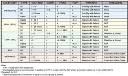
Fortunately, such extreme measures are not required. Simply sorting the various power, control, and signal leads based on their frequency, amplitude, and timing into compatible categories and spatially isolating these categories are all that is necessary. Doing that results in the following circuit categories detailed in Figure 3, which summarizes the information from MIL-HDBK-83575:
� Power and Control DC and AC Circuits
� High-Level Digital and Analog Circuits
� Low-Level DC, AC, and Digital Circuits
� Electro Explosive Devices (EEDs)
� RF/High-Frequency AC and RF Signals
A simple design rule of thumb based on frequency is to use:
� Twisted pair (TP) from circuits with frequencies less than 100 kHz.
� Shielded twisted pair (STP) for circuits with frequencies from 100 kHz to 10 MHz. Depending on the design, STP can be used for circuits with frequencies through 1 GHz. For low-impedance circuits, STP generally is better than coax. However, the EMC characteristics must be individually determined for these circuits.
� Coaxial cable for RF and digital circuits with frequencies greater than 10 MHz.
Figure 3. MIL-HDBK-83575 Wire Harness Categorization
Click here to see larger image
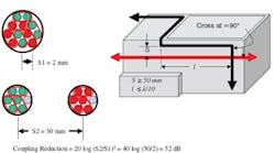
It still is necessary to provide spatial separation between the various categories, and the 2-inch spacing rule is used (Figure 4).
Figure 4. Cable Installation to Minimize Coupling
The figure also illustrates the advantage gained by spacing the categories farther apart. Following the wiring and cable design rules shown in Figures 3 and 4 should eliminate EMC-related installation problems.
But unfortunately, Murphy�s law applies. As a result, there needs to be a contingency plan. And it is not likely that there will be much support to redesign the system to solve what the misinformed believe to be a wiring problem�even if redesign is needed.
Contingencies
Contingency planning will be restricted to what can be done external to the system:
� Add a frequency or amplitude filter to the I/O and connect the cable to the filter. Although there are manufacturers of such devices for standard interfaces, if the system has a nonstandard interface, this may have to be an expensive custom item.
� Run the cable through one or both ends of a split ferrite. This very popular solution works especially well for low-impedance power cables.
� Shield the cable. If it�s already shielded, improve the shielding. As long as the system�s manufacturer controls the cables, this is a great solution. For fixed installations, if cable flexibility is not an issue, conduit is the best cable shielding solution available. Heavy-wall steel conduit has more than 120-dB attenuation for frequencies >5 kHz.
� Replace the cable with electro-optical converters and a fiber-optic run. This is drastic and expensive, but it works. Linear optical performance is an issue, so this approach is better suited to digital data than analog signals.
Filters are a problem, and they are best used directly on the PCBs where they are needed. This is true whether we are discussing the addition of series resistors, series inductors such as ferrite beads, shunt capacitors, LC filters, or diode clamps.
Unfortunately, any time a component is introduced into a high-speed circuit, it generally affects the high-speed operation by changing either L or C. As indicated in the following equation, propagation delay Pd is a function of L and C and increasing either one adds delay:
Propagation Pd = [(L+
?L)(C+?C)]0.5
Additionally, the added L or C lowers the cutoff frequency of the low-pass filter formed by the wiring and cable. Even if there is no more delay, adding a component always reduces the reliability of the circuit and its associated MTBF.
Shielding is an exception. Because it is not placed in the circuit and the cable-shielding envelope generally is spaced far enough from the wiring that the capacitive coupling to ground can be ignored, it does not affect the reliability of the system.
As a suppression technique, shielding also is unique. The other suppression components inserted into the circuit path generally are low-pass filters used to attenuate high-frequency RF current and reduce the radiation at these higher frequencies.
The shield encloses the largest of the radiated emissions source or susceptible circuit pickup elements without being placed directly in the signal or power distribution path. This means that shielding works better at the higher frequencies while filters perform better at the lower frequencies. Because it is not possible to filter the intentional signals, shielding combined with filters generally is the best approach.
Summary
In the normal course of performing their intended function, power and interconnect wiring can act as transmit or receiving antennas and unintentionally couple signals through radiation to other collocated systems and equipment. Wire and cable categorization, isolation, separation, and shielding can be used to reduce these RF coupling effects. Problem solving requires understanding the fundaments of coupling and formulating a systematic approach to handling the different categories of wiring and routing accompanied by a contingency plan.
About the Author
Ron Brewer currently is a senior EMC/RF engineering analyst with Analex at the NASA Kennedy Space Center. The NARTE-certified EMC/ESD engineer has worked full-time in the EMC field for more than 30 years. Mr. Brewer was named Distinguished Lecturer by the IEEE EMC Society and has taught more than 385 EMC technical short courses in 29 countries and published numerous papers on EMC/ESD/PCB and shielding design. He completed undergraduate and graduate work in engineering science and physics at the University of Michigan. e-mail: [email protected]
August 2007


