Cost of Test Reduction Through Optimized Asset Utilization
System-on-a-chip (SoC) unit volume shipments continue to increase at a faster rate than SoC revenues. This compression results in continued pressure to increase throughput and reduce costs in the area of semiconductor test.
Concurrent test and multisite test have long been effective strategies in minimizing the cost to test ICs, and test engineers can utilize methodologies to determine the most cost-effective allocation of resources using both of these strategies.
Concurrent test means testing multiple features or blocks of an individual DUT at the same time. These blocks can be of the same or different functionality. Planning a concurrent test strategy can be a complex task.1 Typically, each block must be tested with instrument channels that are independent of those used for other blocks. This can be a significant restriction if the DUT requires a specialized lower density (that is, scarce) instrument.
Multisite test means testing multiple DUTs at the same time. Again, each site must be tested with its own independent set of instrument channels.
This puts the concurrent test strategy and multisite strategies in contention for the same limited instrument channels. The test engineer is challenged to apportion instrument channels to maximize throughput and minimize cost of test.
A DUT model that is representative of an eight-channel SQUIB driver IC consisting of 16 FET switches serves as an example throughout this article. A SQUIB is an explosive charge that, when detonated, can deploy an automotive safety airbag. Every two channels share a power supply and ground.
While digital and time measurement instruments also will be required to test this device, the focus will be on the relatively more scarce power DCVI instrument. The group of parameters typically tested for each FET includes RDSon, thresholds, timing, leakage, and breakdown. This group will be treated here as one test block.
Another block of tests called firing current tests exercises a high-side FET and a low-side FET connected to either side of a load representing the SQUIB as a system. All test times have been normalized. While they are relatively representative, they do not reflect actual test times of any particular device.
The test system is a simplified model consisting of a 14-slot test head which is filled out as follows:
- Two slots containing instruments to support DUT digital and low-power DC
- Four slots each containing a four-channel power DCVI
- Five slots of instruments required to support other devices
- Two empty slots
- One system support board
The planning will begin with a serial test plan, move to a single-site concurrent test scenario, and then iterate through four plans of sharing and moving scarce resources from concurrent test to multisite test strategies.
Test Concept Planning
Many strategies can minimize the overall cost of testing an IC. The focus will be on the instrument channel allocation challenges of balancing concurrent test and multisite test strategies.
Baseline Serial and Maximum Concurrent Test Plan
Step1: Establish a Baseline Serial Test Time Estimate for the DUT
The serial test time (STT) estimate will focus on the setups, stimuli, and measurements required to implement each test of the specification. It also will serve as a baseline test estimate from which subsequent steps can be derived.
Step 2: Assess DUT Opportunities and Restrictions for Concurrent Test
The DUT features and functionality may impose restrictions that prevent certain blocks from being tested concurrently. In this example, it is assumed that all 16 individual FETs can be tested concurrently but not at the same time as the firing current tests.
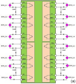
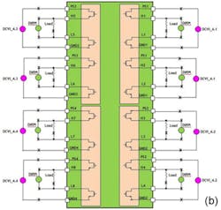
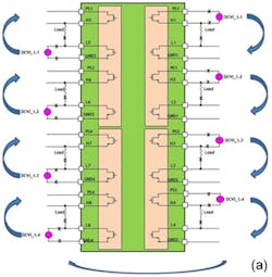
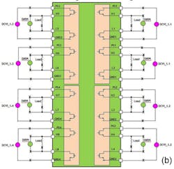
Based on this, DCVI instrument channels are assigned to DUT pins as shown in Figures 1a and 1b. There is a DCVI channel dedicated to each FET and to each pair of driver channels. Low-side FETs require more testing and have longer test times than high-side FETs. Firing current tests can be implemented for all eight DUT channels concurrently. For an actual device, power dissipation limitations may restrict the number of FETs that can be tested concurrently.
Step 3: Calculate the Ideal Concurrent Test Time
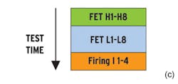
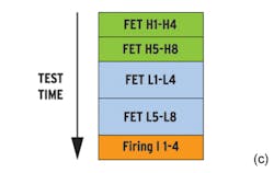
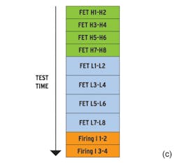
The Ideal Concurrent Test Time (ICTT) is made up of two parts: the sum of test times for blocks that cannot be tested concurrently and the longest test time of the blocks that can be tested concurrently. In this example, all of the individual FETs can be tested concurrently. The low-side FETs take longer to test than the high-side FETs and therefore determine the test time of this block of tests (b). Figure 1c shows this test flow.
Figure 1. Eight-Channel SQUIB Driver with Concurrent Test FET Blocks (a), Concurrent Test Firing Circuit (b), and Ideal Concurrent Test Flow (c)
Step 4: Estimate the Maximum Achievable Concurrent Test Time (CTT)
The test system architecture could add some overhead test time to the individual block test time when testing concurrently with others; for example, if the test system does not support broadcast instrument setups or asynchronous threshold tests. The overhead can be estimated from previous test solutions and refined during the test development phase of the current project. For illustrative purposes, a 3% overhead is used in this example. It is useful to calculate the Concurrent Test Efficiency (CTE)2 for this step:
where: STT = STT estimate from Step 1
ICTT = ICTT from Step 3
CTT = maximum achievable test time from Step 4
Step 5: Tabulate the Cost of the Test System, Handler, and DIB Required to Support the Maximum Achievable Concurrent Test Time Scenario
Step 6: Calculate the Cost of Test
Multisite Test Plan
Expanding the test plan to include multiple sites requires additional considerations:
- Is there room on the DIB for additional contactors, loads, relays, etc., to support additional sites?
- Will the handler need to be upgraded to support multiple devices?
- Are sufficient instrument resource channels available to support additional sites?
The focus will remain here on the instrument channel availability. In the example so far, all four of the DCVI instruments have been used to support concurrent test. There are no more DCVI available to support even one more site. DCVI instrument channels must be identified to support additional sites. At this point, there are some choices to consider:
- Can the DCVI channels be fanned out?
- Can any of the scarce power DCVI channels be replaced by higher density instruments?
- Can DCVI channels be added to the tester?
- Can the DCVI channels be shared by switching among DUT pins?
- Can the switching be implemented by test system mux's and buses?
- Will the DIB real estate accommodate additional switching?
Assume that fan-out is impractical and that higher density instruments cannot be substituted due to the power requirements of the tests. There are two empty slots that could hold two additional DCVI instruments. However, this would be insufficient to support even one additional site with this maximum concurrency scenario. It will be necessary to share DCVI channels among DUT pins. Instrument channels that are switched among DUT blocks cannot be used concurrently to test those blocks. Moving instruments from dedicated to shared will reduce the CTE. If this frees up instruments to support additional test sites, the overall impact on the cost of test may be positive.
Shared Resource Plan A: Three Sites
The following steps provide a logical, iterative approach to finding the best balance of resource channel allocation to achieve the lowest cost of test.
Step 1: Identify Concurrently Tested DUT Blocks that Could Share DCVI Channels
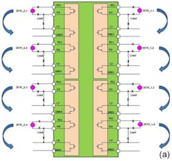
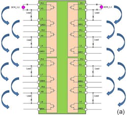
Since sharing DCVI channels will negatively impact CTE, this should be an incremental step in determining the ultimate impact of cost of test. In the first step, DCVI_1 and DCVI_2 will be used to test all eight high-side FETs concurrently. DCVI_1 and DCVI_2 then will be switched to test all eight low-side FETs concurrently. Finally, DCVI_1 will be switched to test all four firing current channels concurrently. The instrument channel assignment is shown in Figures 2a and 2b. Note that the number of DCVI instruments required to test a single site has been reduced to two. Two DCVIs now are free to support an additional site. Adding two DCVIs to the empty slots would support an additional site for a total of three sites. The test flow now is shown in Figure 2c.
Figure 2. Shared Plan A FET Blocks (a), Shared Plan A Firing Circuit (b), and Shared Plan A Test Flow (c)
Step 2: Calculate the Single-Site Test Time Based on the New Flow as Shown in Figure 2c
Switching time is likely small but can be added to the single-site time. Calculate CTE using this single-site test time as the new CTT.
Step 3: Calculate the Time that It Will Take to Test All Three Sites and the Effective Parallel Test Time per Site
This is done by applying an expected parallel test efficiency factor to the single-site test time estimate and then dividing that time by the number of sites:
where: N = number of sites
T1 = single-site test time
PTE = expected parallel test efficiency
TN = time to test all three sites
Effective Parallel Test Time Per Site = TN/N.
PTE is estimated based on previous experience and can be refined during the test development phase. It can be a single estimate if known with some confidence, or it can be a range of expected PTE. A range will be used in this example.
Step 4: Tabulate the Cost of the Test System, Handler, and DIB Required to Support the Shared Resource Plan A Scenario
In this case, it is assumed that the handler required to handle multisite testing will be more expensive and that the DIB will be more complex and more expensive.
Step 5: Calculate the Cost of Test for Each of the PTE Estimates
Step 6: Plot Cost of Test vs. PTE for Shared Resource Plan A Scenario
Identify this curve with the CTE and site count for this scenario.
Shared Resource Plan B: Six Sites
Identify the next group of concurrently tested DUT blocks that could share DCVI channels. In this case, a single DCVI is shared among all FETs and the firing current tests. This results in five free DCVIs that can support five additional test sites. Steps 2-7 from Plan A then are followed to plot cost of test vs. PTE for this scenario. The resource sharing and test flow are shown in Figure 3a, b, and c.
Figure 3. Shared Plan B FET Blocks (a), Shared Plan B Firing Circuit (b), and Shared Plan B Test Flow (c)
Shared Resource Plan C: Eight Sites
Identify the next group of concurrently tested DUT blocks that could share DCVI channels. In this case, two channels of a single DCVI are shared among all FETs and with the firing current tests. This results in 22 free DCVI channels. If the handler and/or DIB real estate limits the site count to eight, 14 of the free channels could be used to support seven additional sites. The remaining eight free channels (two DCVI instruments) could be removed from the tester configuration to reduce capital costs. Steps 2-7 from Plan A then are followed to plot cost of test vs. PTE for this scenario. The resource sharing and test flow are shown in Figure 4a, b, and c.
Figure 4. Shared Plan C FET Blocks (a), Shared Plan C Firing Circuit (b), and Shared Plan C Test Flow (c)
Shared Resource Plan D: 12 Sites
This is the same resource sharing plan as Plan C but assumes that the handler and DIB real estate can support 12 sites. The two DCVIs removed in Plan C are returned to the configuration to support the additional sites. Steps 2-7 from Plan A then are followed to plot cost of test vs. PTE for this scenario.
Results
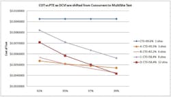
Results are summarized in Figure 5 and Table 1. Test-system cost and DIB cost have been combined and normalized to the figure called ATE $. The handler cost has been normalized to the figure called Handler $.
Figure 5. Results Summary
Table 1. Results Summary
(Click on the table to view a larger copy of the image)
Limitations and Discussion
A relatively simple example was used to allow better focus on the process. Depending on the actual device architecture, this model could be extended to cover a more complex device or applied incrementally to separate blocks that share a common scarce resource.
As the site count expands, it is possible that even the higher density DC and digital instrument channels may become scarce. The same strategy described for the DCVI then could be applied to these channels as well.
Test-time estimate accuracy is at the same time crucial and difficult to achieve. Historical data from previous similar devices can help. It also can help to break down tests into common subcategories of actions that can be more easily estimated.
CTE and PTE estimates can be accommodated by historical data and refined as the test development process proceeds. In this example, a single CTE value was used to reflect concurrent test inefficiency regardless of the number of blocks tested at the same time. There may be some value in using a different CTE to reflect more or fewer concurrent blocks.
DIB real-estate limitations can restrict the number of sites tested at the same time. This may be alleviated in the special case of index parallel test. If the test system can support running multiple copies of the test program and if device packaging will accommodate strip handling or turret handling, then test sites can be separated to multiple physical locations (DIBs).
Device functionality or characteristics can restrict concurrent test of different blocks. Again, this problem may be alleviated by using the index parallel test. In this case, though, the test system must be able to run different test programs at the same time. For example, all of the high-side FETs could be tested at one test site while all of the low-side FETs are tested at a second site and all firing current tests are tested at a third site.
As a database is built from testing similar devices, test time and efficiency estimates can be refined. With enough experience, this process could be truncated or abbreviated.
Typically, resources are shared within a site while sharing across sites is avoided if possible. This may not always be the most cost-effective choice as shown in this two-site example. The DUT includes two separate blocks, A and C, that can be tested concurrently. Each block requires a digitizer. The number of digitizer channels required for concurrent test across two sites then is four.
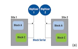
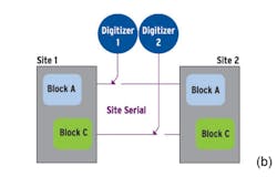
In this example, only two digitizers are available which means that they must be shared. Block-serial sharing is indicated in Figure 6a where each digitizer is dedicated to a site and shared between Block A and Block C. Site-serial sharing is indicated in Figure 6b where each digitizer is dedicated to a block and shared between sites.
Figure 6. Block Serial Sharing (a) and Site Serial Sharing (b)
In Figure 7a, the test times of Block A and Block C are equivalent. In this case, block-serial and site-serial sharing would result in similar test times. However, if Block A test time is significantly longer than Block C test time, block-serial sharing would result in a significant test time savings over site-serial sharing. This is shown graphically in Figure7b.
Figure 7. Equivalent Block A and C Test Times (a) and Long Block A Test Time (b)
Conclusions
An iterative planning progression can result in a cost-effective allocation of scarce resources that may not have been otherwise obvious.
For example, Plan B (six sites) does not overcome the CTE advantage of Plan A (three sites) until PTE reaches ~95%.
Plan C achieves the lowest capital cost as a result of reduced configuration but has the highest cost of test of the shared resource plans.
The choice to share a resource between sites or between blocks within a site is dependent on the relative test times of the blocks.
Acknowledgements
I would like to thank Tom Chambers, Randy Kramer, Rick Nohelty, Jacques Vieuxloup, Bethany Van Wagenen, and Massimo Zambusi for their ideas and contributions.
References
1. Van Wagenen, B. and Seng, E., “Concurrent Test Planning,” Proceedings, International Test Conference 2010, IEEE Computer Society, November 2010.
2. Kramer, R., “Exploring Concurrent Test Efficiency,” EE-Evaluation Engineering, July 2010, pp. 44-47.
About the Author
John Wilcox is a factory applications engineer at Teradyne. He started working at Teradyne in the area of functional laser trim before moving to mixed- signal applications. He also has held positions as a field applications engineer and applications engineering manager. Wilcox received a B.S.E.E. from the University of Illinois. [email protected]

